IMEC
IMEC is a global research center focused on nanoelectronics, photonic systems, and sustainable energy technologies. As a leader in semiconductor R&D, IMEC is driving advancements in AI, 5G, and advanced materials. With collaborations with industry leaders and academic institutions, IMEC is pushing the boundaries of electronics research, supporting the development of next-generation technologies. From quantum computing to photonic integrated circuits, IMEC’s innovations are shaping the future of electronics, communications, and sustainability, positioning the organization as a key player in the global technological ecosystem.
Posted on 27th March 2026 | Modified on 28th March 2026
AI, Business, Research
Imec has given Jensen Huang, founder and CEO of Nvidia, its 2026 Lifetime of Innovation Award. The honour recognises Huang’s instrumental role in enabling accelerated computing technologies and empowering critical AI applications across industries – fuelled by the invention of the GPU. The award ceremony, including a video interview with Huang, will be held on 19 May, during imec’s ITF ...
Posted on 26th March 2026 | Modified on 26th March 2026
Latest news
What caught our eye these last seven days? Imec getting the world’s most advanced litho tool, Arm taking on Intel with a proprietary server CPU, and SWISSto12 3D printing GEO satellites...
Posted on 20th March 2026 | Modified on 24th March 2026
Business, Research
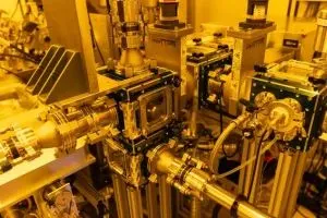
Imec has received the ASML EXE:5200 High NA EUV lithography system, said to be the most advanced lithography tool available today. The tool gives imec’s partners early access to the next generation of chip-scaling technologies. Integrated directly with a comprehensive suite of patterning and metrology tools and materials, the High NA EUV system will empower imec and its ecosystem partners ...
Posted on 17th March 2026 | Modified on 17th March 2026
Business
Imec has launched a consortium with 26 European university groups that will work on the technology roadmap beyond CMOS scaling (CMOS 2.0). This initiative will focus on design automation and chip architecture research. The consortium will benefit from the NanoIC pilot line, turning academic insights into industry-focused innovations. Similar consortia will be set up around advanced materials and alternative compute ...
Posted on 11th March 2026 | Modified on 11th March 2026
Business, Research
Cornell University researchers have used high-resolution 3D imaging to detect atomic-scale defects in ICs. The imaging method was the result of a collaboration with TSMC and ASM and the research was funded by TSMC. Tiny defects have been a long-standing challenge for the semiconductor industry. The game-changer is electron ptychography, a computational imaging method in which an electron microscope pixel ...
Posted on 6th March 2026 | Modified on 6th March 2026
Business, Research
Imec and Atlas Data Storage, a specialist in production-scale DNA data storage, have joined forces to to accelerate the development of digital data storage using synthetic DNA. The collaboration combines Atlas’ ASIC design expertise and scalable DNA synthesis technology with imec’s expertise in advanced chip development, fabrication, and integration. In addition to prototyping and strategic support, imec is investing in ...
Posted on 26th February 2026 | Modified on 26th February 2026
Business, Research
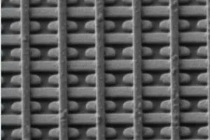
Imec has demonstrated that precise control of gas compositions during post-exposure EUV lithography steps can help in minimizing the required exposure dose, thereby unlocking higher wafer throughput. In particular, improved dose response of metal-oxide photoresists (MORs) has been achieved when the EUV post-exposure bake step is performed under elevated oxygen concentrations. Metal-oxide resists (MORs) have emerged as leading candidates for ...
Posted on 18th February 2026 | Modified on 18th February 2026
Business, Power Supplies, Research
Imec has unveiled a 7‑bit, 175GS/s ADC that combines a record-small footprint (250 x 250µm²) and low conversion energy with one of the fastest sampling speeds ever reported. As such, the ADC meets the rapidly increasing throughput and processing demands of AI- and cloud-driven datacentres, without the area and power explosion typically seen at ultra-high sampling rates. Driven by AI and ...
Posted on 4th February 2026 | Modified on 4th February 2026
Business, Research
The NanoIC pilot line, a European initiative coordinated by imec and dedicated to accelerating innovation in chip technologies beyond 2nm, announces the release of two new process design kits (PDKs): an A14 pathfinding PDK for advanced logic scaling and an eDRAM system exploration PDK for advanced memory innovation. Both PDKs are first‑of‑their‑kind releases, providing early access to cutting-edge design rules and ...
Posted on 28th January 2026 | Modified on 28th January 2026
Business, Research
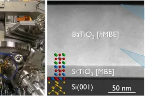
Veeco Instruments and imec have developed a 300mm high volume manufacturing compatible process that enables the integration of barium titanate (BaTiO3 or BTO) on a silicon photonics platform. At present, there is no commercially available production-compatible solution for manufacturing these materials. BTO is a promising material with unique electro-optical properties that can be used for high-speed and low-power light modulation ...
 Electronics Weekly