Electronics Weekly
These early-access PDKs bring advanced packaging capabilities within reach of universities, start‑ups, and industry innovators.
By enabling chiplets to be interconnected at high density, advanced packaging provides the foundation for the next generation of high‑performance computing, AI accelerators, and data‑intensive applications.
The RDL PDKintroduces a new way to achieve high‑density chip‑to‑chip connections using polymer‑based substrates.
Traditionally, these substrates could not support extremely fine lines, limiting their use in advanced packaging. Imec’s technology, developed within the NanoIC project, overcomes this barrier by enabling exceptionally small‑pitch interconnects in a polymer‑based RDL, offering capabilities that go beyond what leading commercial fabs provide today.
With line widths and spaces down to 1.3 microns and microbump pitches as tight as 20 microns, the RDL PDK gives designers access to interconnects that can improve communication speed by up to 40% and reduce energy per bit by as much as 15% on a UCIe-Advanced die-to-die interface.
As a result, fine‑pitch RDL becomes an appealing integration option for a wide range of emerging applications, from automotive and high‑performance computing to next‑generation GPU architectures.
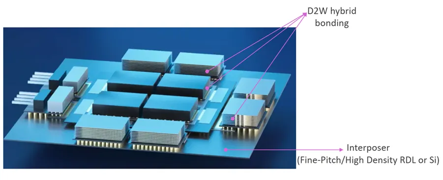
The D2W PDK: enables extremely compact, direct connections between dies using the third dimension.
Instead of relying on traditional copper bumps, hybrid bonding forms direct oxide‑to‑oxide links between the CMOS die and the package interface. This eliminates the parasitics associated with copper bumping and enables low‑loss, energy‑efficient communication pathways.
With its ability to create ultra‑dense, high‑bandwidth chip‑to‑chip links, the D2W hybrid bonding PDK is particularly suited for AI applications, advanced computing platforms, and high‑performance GPU architectures.
With this release, imec becomes the world’s first to offer easy‑access interconnect PDKs at these integration levels and dimensions. This initial “exploratory version” provides the essential tools designers need to begin assessing the technology: systematic layout creation, automated and custom routing, and design rule checks.
“Th. All practical details are available on the NanoIC website.