Electronics Weekly
ZAM, a stacked DRAM alternative to HBM with a claimed 40-50% power advantage and 2x-3x density advantage over HBM, is the product of a jv between Softbank, Tokyo University and Intel called Saimemory which was later joined by Fujitsu.
The initial technology came from Intel, Tokyo University and other Japanese academic sources. ZAM development is expected to cost $70 million. Softbank is putting up $21 million.
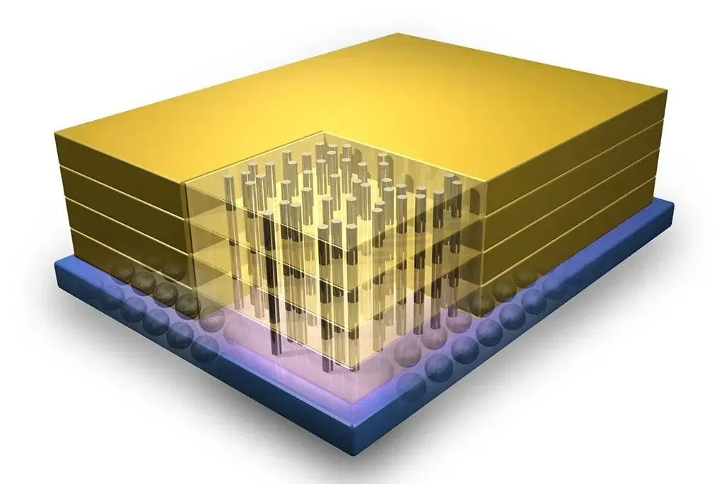
ZAM gains its thermal advantage from architectural and packaging innovations.:
Unlike HBM, which uses straight vertical TSVs, ZAM uses diagonal interconnects that route connections at an angle within the die stack which shortens signal paths and reduces electrical resistance.
ZAM uses a hybrid copper-to-copper bonding method that eliminates solder bumps. This creates a “monolithic” silicon block, lowering the energy needed for data to travel between layers.
By removing the central TSV field, the solid silicon centre acts as a vertical heat spreader. This improved heat conduction reduces leakage allowing the memory to operate more efficiently at lower voltages.
The modules will be capacitor-free and for integration with AI chips, EMIB technology will be used, which provides a high-speed connection between individual crystals using a thin silicon bridge embedded in the substrate of the case which minimises the energy consumed during data transfers.
Shinko Electric Industries and Powerchip Semiconductor are contributing manufacturing and prototyping. Intel will provide the stacking technoloy..
Another company pursuing the same approach is NEO Semiconductor.
Nvidia recently paid Groq $20 billion for AI inferencing IC technology which eliminates the need for HBM.