Electronics Weekly
The technology approach will also be rebranded to Rapidus AI-Agentic Design Solution with multiple tools being released starting in 2026 and will be provided to customers together with a process design kit and reference flows. The new tools include:
- Raads Generator: an EDA tool based on large-scale language models. When designers input semiconductor specifications, Raads Generator outputs register-transfer level (RTL) design data optimised for Rapidus’ 2nm manufacturing process.
- Raads Predictor: a tool for RTL debugging and optimisation for physical design, placement and routing. Raads Predictor will provide a power performance area (PPA) estimate in a short period of time.
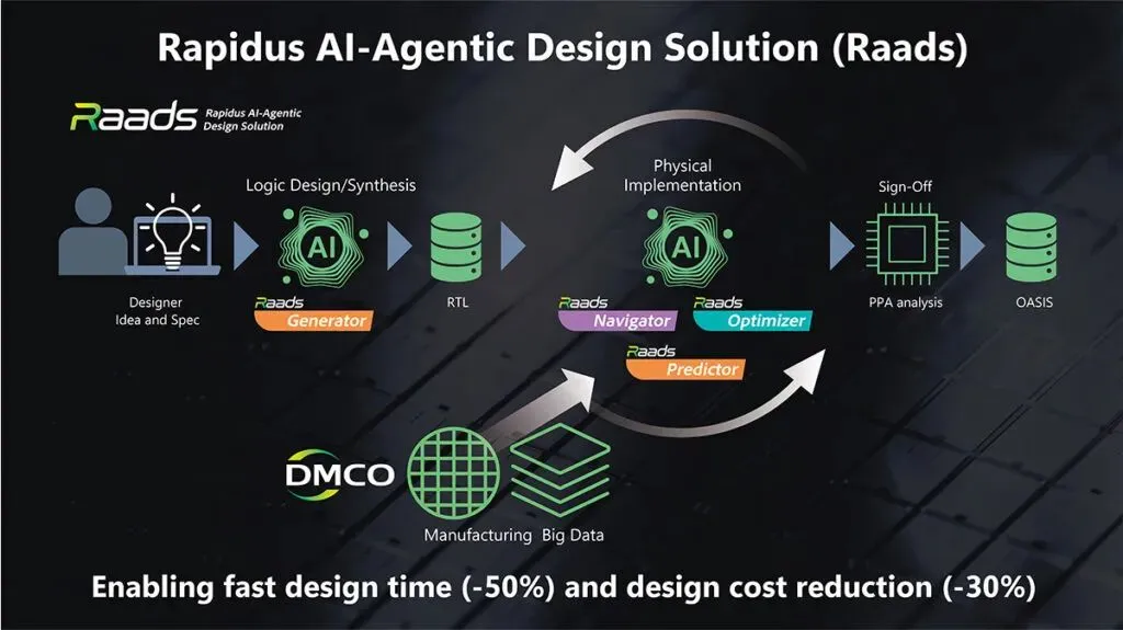
Designers can use Raads Generator to write design ideas and desired specifications as RTL source code and then input data into Raads Predictor along with Synopsys Design Constraints, allowing them to predict the PPA of the silicon manufactured by Rapidus.
Raads not only assists semiconductor designers with AI but will also become an AI agent for cutting-edge semiconductor device design. By utilising Raads in conjunction with existing EDA tools, developers can reduce design time by 50% and design costs by 30%.
Following the launch of Raads Generator and Raads Predictor, Rapidus will also release additional tools throughout 2026 including:
- Raads Navigator/ Raads Indicator: utilises LLMs to provide quality assurance and assistance to designers to derive solutions to design issues and problems.
- Raads Manager: a layout design tool that utilises ML/AI to create a hierarchical configuration that minimises design time.
- Raads Optimizer: applies ML/AI to search for and derive parameters to optimise PPA.
Rapidus’ Innovative Integration for Manufacturing (IIM-1) foundry is introducing a single-wafer processing for all manufacturing processes.
In June 2025 Rapidus connected 200 pieces of semiconductor manufacturing equipment to enable a completely new automated material handling system to support 2nm GAA prototyping.
In July Rapidus announced that prototyping had started at IIM-1 and the prototype wafers started to obtain their electrical characteristics.