Electronics Weekly
Keysight’s semiconductor parametric tester technology, analysis solution and expertise in semiconductor manufacturing process optimisation will advance Rapidus’ Design-Manufacturing Co-Optimization (DMCO) concept.
The two companies will identify the factors that contribute to improving PDK accuracy, including the research methods and technologies, to clarify the magnitude of their impact and then consider how to realise and implement these methods.
 In parallel, the companies will also carry out similar efforts to identify factors that contribute to improving the performance of semiconductor elements, circuits and factors that improve the yield of the wafer process.
Keysight has developed and commercialized original analysis algorithms and comprehensive, versatile data formats or process control monitoring to optimize semiconductor processes, improve yields and solve various on-site problems.
Leveraging this new data format and analysis algorithm, Keysight is commercializing a new root-cause analysis solution, the Keysight Wafer Operations Analytics Suite, which aims to identify the individual root causes of various problems, thereby contributing to improved semiconductor design and manufacturing quality and cost reduction.
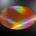
Rapidus began prototyping 2nm gate-all-around (GAA) transistors at its development facility in Chitose City, Hokkaido called Innovative Integration for Manufacturing (IIM-1).
Rapidus is currently building its Rapid and Unified Manufacturing Service (RUMS), a new semiconductor foundry concept which will introduce a single-wafer process for all manufacturing processes to achieve short turnaround time.
Data acquisition of various semiconductor parameters has already begun. Data from parametric testers will be analysed using Keysight’s root-cause analysis solution to identify the causes of various manufacturing issues.
Rapidus will use data acquired by both companies at the manufacturing site to develop a PDK compatible with Rapidus’ 2nm GAA manufacturing process.