Posted on 20th March 2026 | Modified on 24th March 2026
Business, Research
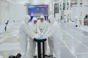
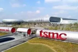
Imec has received the ASML EXE:5200 High NA EUV lithography system, said to be the most advanced lithography tool available today. The tool gives imec’s partners early access to the next generation of chip-scaling technologies. Integrated directly with a comprehensive suite of patterning and metrology tools and materials, the High NA EUV system will empower imec and its ecosystem partners ...
Posted on 26th February 2026 | Modified on 26th February 2026
Business, Research
Imec has demonstrated that precise control of gas compositions during post-exposure EUV lithography steps can help in minimizing the required exposure dose, thereby unlocking higher wafer throughput. In particular, improved dose response of metal-oxide photoresists (MORs) has been achieved when the EUV post-exposure bake step is performed under elevated oxygen concentrations. Metal-oxide resists (MORs) have emerged as leading candidates for ...
Posted on 24th February 2026 | Modified on 24th February 2026
Business, Manufacturing
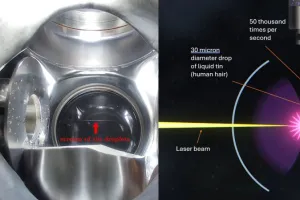
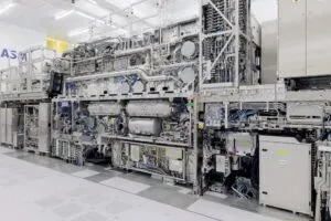
ASML has developed a 1000W light source which should increase the throughput of its high-NA EUV machine from 220wph to 330wph by 2030. The advance has been achieved by doubling the rate at which the molten tin drops in an EUV machine are exposed to a CO₂ laser beam to create plasma that emits EUV radiation. By doubling the droplet ...
Posted on 17th October 2025 | Modified on 22nd October 2025
Business, Manufacturing
Samsung is reported to be paying $773m for two high-NA EUV machines – the Twinscan EXE:5200B – with one for delivery this year and one for delivery in H1 2026. Samsung already has a high-NA EUV tool for R&D use at its Hwaseong facility, which is where the two new high-NA machines will also be installed. The two machines will ...
Posted on 26th September 2025 | Modified on 26th September 2025
Latest news
Our most read stories cover a compact fan-less AI edge computer, the fast growth of the automotive chip market, and Imec advances around EUV lithography...
Posted on 25th September 2025 | Modified on 25th September 2025
Latest news
This week we're talking about an AI investment bubble, high numerical aperture EUV lithography, and in-orbit construction...
Posted on 22nd September 2025 | Modified on 22nd September 2025
Research
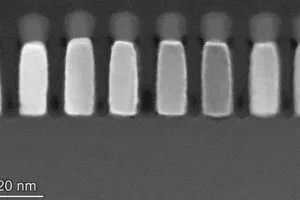
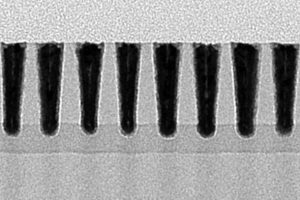
Belgian research lab Imec has revealed advances single-print high numerical aperture EUV lithography at the ‘SPIE Photomask Technology + EUV Lithography’ conference in Monterey California: Line structures at 20nm pitch with 13nm tip-to-tip CD (critical dimension) – relevant for damascene metallisation Electrical test on 20nm pitch ruthenium lines obtained using direct metal etch From the left: 20nm pitch line structures ...
Posted on 5th September 2025 | Modified on 7th September 2025
Business
SK Hynix has become the first memory manufacturer to install ASML’s next-generation High-NA Extreme Ultraviolet (EUV) lithography system. The installation of the Twinscan EXE:5200B at its M16 fab in Icheon, South Korea, positions SK Hynix to simplify manufacturing processes and accelerate the development of future DRAM chips for the AI and computing markets. Technical and production impact Resolution and density: ...
Posted on 24th February 2025 | Modified on 25th February 2025
Research
Belgian research lab Imec has revealed test results from 20nm pitch metal lines patterned using a single-exposure of high NA (numerical aperture) EUV lithography. Top-down SEM pictures of 20nm pitch meanders after pattern transfer into TiN hard mask Metal oxide negative tone resist was used, and yield was over 90%. “This is the first ever electrical yield demonstration of 20nm ...
Posted on 27th December 2024 | Modified on 24th December 2024
Manufacturing
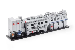
ASML is used to having customers clamouring for its the photography machines during chip booms when supply is tight but sales of its latest offering is being restricted by the company’s own choice. A Lego model (pictured above) of ASML’s $350 million High-NA EUV machine is on sale in the company store for €208. Despite widespread interest in obtaining a ...
 Electronics Weekly