 Electronics Weekly
Make sure to listen to the latest episode of the excellent Electronics Weekly podcast, CHIIPS. It features Joe Stockunas, president of SEMI Americas.
CHIIPS #19 – Semiconductor industry insights from Joe Stockunas of SEMI Americas

Make sure to listen to the latest episode of the excellent Electronics Weekly podcast, CHIIPS. It features Joe Stockunas, president of SEMI Americas.
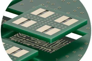
A multi-domain passive module with functionality embedded in the substrate has been developed by Saras Micro Devices. The Saras Tile, or STILE, enables power regulation from system board to package. Saras’ approach is for vertical power delivery to reduce parasitic losses. Stacking the power stage and passive components in line with the die shortens the power path and reduces parasitic ...
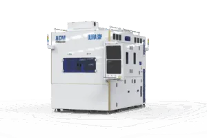
The Ultra ECDP (electrochemical deplating) tool is designed specifically for wide bandgap compound semiconductor manufacturing, said ACM Research. It delivers uniform processing outside of the wafer pattern area with minimal undercut for high-precision wafer level gold (Au) bump, thin film and deep hole deplating. Gold exhibits high conductivity, corrosion resistance and malleability and is emerging as an advantageous material for ...
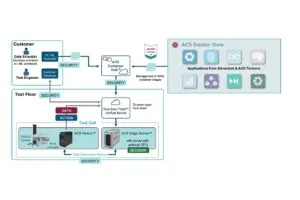
The ACS RTDI (Advanced Cloud Solution RealTime Data Infrastructure) software uses AI to test advanced chips, says Advantest. It uses low-latency edge computing and analytics to monitor complex semiconductor. The algorithms can provide analysis, corrective analysis and prompt actions to improve quality and yield. Advantest said, semiconductor manufacturers can use AI algorithms and data analytics to extract insights from the ...

A hyper-beam array lithography system has been introduced to the US, based on architecture pioneered in Europe. The lithography tool operates with 65,000 independently controlled parallel beams which delivers capabilities at a scale no electron beam technology can match, said the company. Installed at Northrup Grumann, it addresses the holy grail of chip design, said founder and CEO, Lex Keen. ...

Spending on 300mm fab equipment is expected to reach $107bn in 2025, according to the 300mmm Fab Outlook report by SEMI. The sector is expected to grow 7% this year and 9% in 2026 to reach $116bn, a 4% increase in 2027 followed by a 15% increase and total worldwide expenditure of $138bn in 2028. Over the next three years, ...

There were many changes to the format of Semicon West this year, not least the change of venue to Phoenix, Arizona. The semiconductor, electronics design and manufacturing show had been held in San Francisco and this was the first year of a ‘co-parenting’ arrangement, which will see the conference alternate between the two cities every October. One change that many ...

The semiconductor, electronics design and manufacturing industry association, SEMI, has announced that Greg Barrett will succeed Kevin Bauer as CFO (chief financial officer) and business operations officer. Before joining SEMI, Barrett was senior vice president and CFO of Efinix, a programmable semiconductor company. He also held senior roles at Super Micro Computer, Rambus, Micron Technology and Altera. “Greg’s specialised industry ...
From smartphones and computers to autonomous vehicles and AI, the world’s increasing reliance on these technologies has pushed semiconductor demand to an all-time high. Semicon West is a gathering of leaders across the microelectronics supply chain to explore transformative technologies, develop the future workforce, and drive strategic collaboration. With keynotes, TechTALKs and networking events. Topic areas include cybersecurity, heterogeneous integration, ...