Electronics Weekly
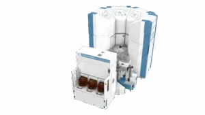
Kinex is an integrated die-to-wafer hybrid binding system, Xtera (pictured) is for GAA (gate-all-around) transistors and PROVision 10 eBeam is a metrology system for 3D chips.
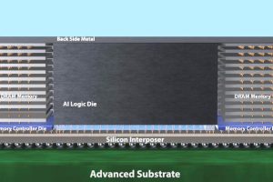
The Kinex bonding system was developed in collaboration with Dutch equipment supplier, BE Semiconductor Industries (Besi). Hybrid bonding uses direct copper-to-copper bonds to enhance a chip’s performance and power consumption and is increasingly specified for GPUs and high performance computing (HPC) chips, said the company. Combining Applied’s front-end wafer hybrid bonder and Besi’s bonding accuracy and speed, Kinex is believed to be the first integrated die-to-wafer hybrid bonder.
Filling the high aspect ratio source/drain trenches of 3D GAA transistors using conventional epitaxial (epi) is challenging, explained the company. It can lead to voids and uneven growth which reduces performance and reliability. The Centura Xtera Epi system is designed for GAA transistors at 2nm and beyond. Its low-volume chamber architecture includes integrated pre-clean and etch processes to enable void-free GAA source-drain structures with 50% lower gas usage than conventional epi, said Applied. The deposition-etch process continuously adjusts the trench opening as material grows on the side walls and bottom of the trench to optimise epi growth across the transistors on a wafer, void free with a greater than 40% improvement in cell-to-cell uniformity, claimed the company.
Finally, to obtain precise measurements and accelerate yield of complex chip designs, the company has introduced the PROVision 10 eBeam metrology system. “The increased use of 3D architectures in logic and memory is creating new metrology challenges that are pushing optical technology to the limits,” said Keith Wells, group vice president of imaging and process control at Applied Materials. The metrology system is built for advanced logic chips, including GAA transistor and backside power delivery architectures , advanced DRAM and 3D NAND chips. According to the company it is the first metrology system to feature cold field emission (CFE) technology, which increases nanoscale image resolution by up to 50% and imaging speed by up to x10 compared to conventional thermal field emission (TFE) technology. Sub-nanometer imaging capabilities allow it to see through multiple layers of 3D chips and provide an integrative, multi-layer image for direct on-device overlay measurements and precise critical dimension (CD) metrology, beyond the limits of traditional optical systems. Its supports EUV layer overlay and nanosheet measurement and epi void detection in GAA transistors, for 2nm and beyond, as well as HBM integration.