Electronics Weekly
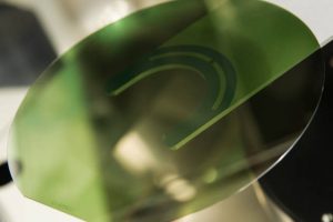
“Due to its material properties, glass offers a promising basis for microelectronics – in particular, its high dimensional stability allows ultra-fine conductor tracks, even below 5μm as structure widths,” according to the Fraunhofer.
The aim is to displace traditional organic substrates when high-bandwidth, high conductor-count communication has to be supported between chips and chiplets.
In particular, the creation of through-glass vias and associated redistribution layers have to be developed to the point that they can be transferred to production.
Proposed technologies will pass though reliability tests, including thermal cycling, moisture sensitivity analysis and vibration analysis to asses readiness for high-volume production.
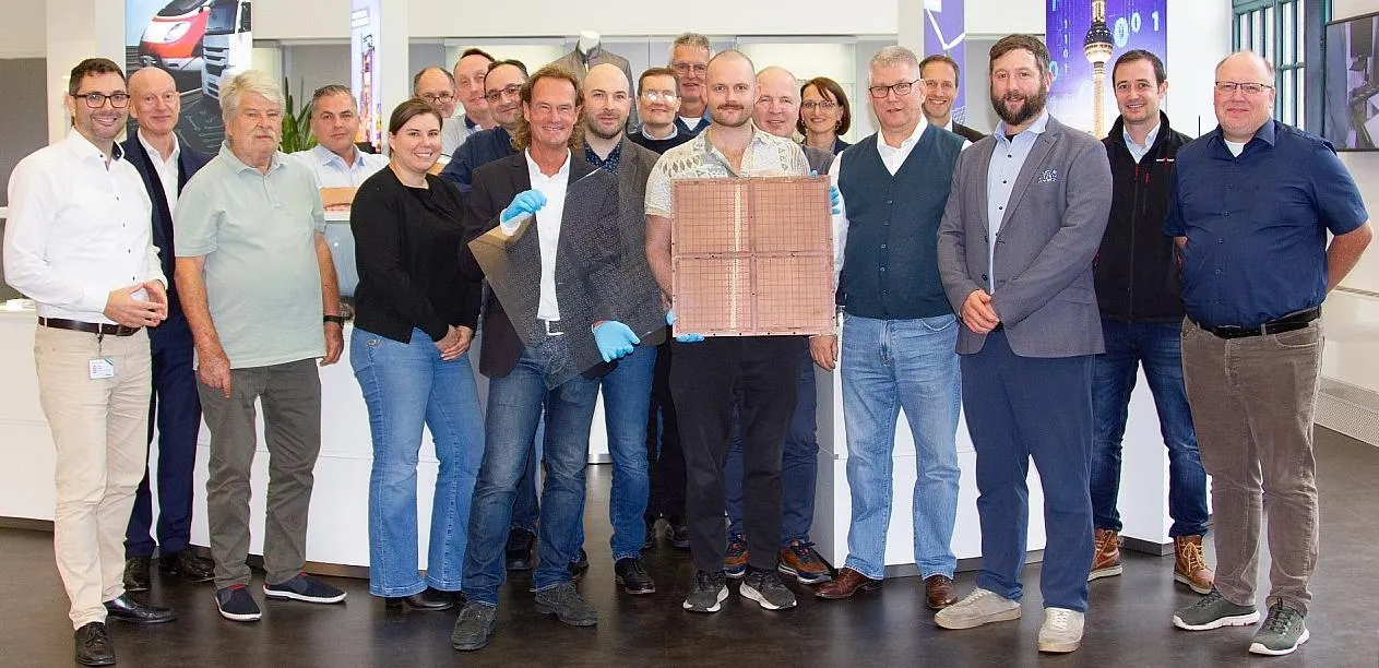
The consortium, to be called ‘Glass panel technology group’, was officially launched at Fraunhofer IZM in Berlin on 1 October.
It has 15 companies and will be led by Fraunhofer IZM.
“The group unites major companies from across the value chain, including material suppliers, manufacturers, and system integrators,” according to member LPKF Laser & Electronics. “The objectives include establishing partnerships for knowledge and technology exchange related to high-volume manufacturing of glass panel technology, developing glass-based substrates on large panel formats, and conducting reliable testing procedures for quality assurance.”
LPKF is bringing laser induced deep etching to the party for drilling through-glass vias.