Electronics Weekly
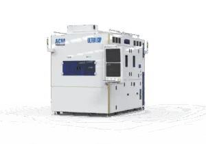
It delivers uniform processing outside of the wafer pattern area with minimal undercut for high-precision wafer level gold (Au) bump, thin film and deep hole deplating.
Gold exhibits high conductivity, corrosion resistance and malleability and is emerging as an advantageous material for compound semiconductors use in EVs, 5G/6G communications, RF and AI, said Dr David Wang, president and CEO of ACM Research. Compound semiconductor manufacture requires the use of substrates with distinct weight, stress and thickness characteristics, such as SiC, GaAs or lithium phosphate. The modular Ultra ECDP tool can integrate both plating and deplating processes and use multi-anode technology to control deplating in different areas. IT also offers horizontal, full-face deplating to prevent cross-contamination during processing.
The Ultra ECDP’s specialised processes include Au bump removal, thin film Au etching, and deep-hole Au deplating, supported by integrated pre-wet and cleaning chambers. Features include precise chemistry circulation and advanced multi-anode electrochemical deplating for minimised side etching and uniformity, added ACM Research.
It is compatible with six- and eight-inch manufacturing and accommodate 150mm, 159mm and 200mm wafer sizes. The system is configurable with two open cassettes and one vacuum arm.
Related Semicon West 2025 news: