Electronics Weekly
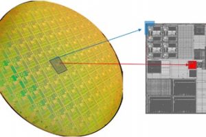
“This demonstrated resolution also meets the industry requirement for the next-generation 14nm and 10nm logic technology nodes,” claimed French research lab CEA-Leti.
So many tricks need to be played to push conventional 193nm lithography below 22nm that the law of decreasing returns – particularly needing multiple masks in each lithography step – is making alternatives increasingly attractive.
Extreme UV is one of those alternatives, although light sources are a nightmare and the technology needs reflective masks, which are exceptionally hard to keep defect-free.
Another proposed alternative is direct-write electron-beam, which has been used for years to make high-resolution one-offs as it easily copes with nanometre resolutions.
It does not need a mask, but it is incredibly slow – completely unsuited to production.
Multi-e-beam schemes have been proposed, and fallen by the wayside.
Now a programme called ‘Imagine’, using 1,000 beam technology from Dutch firm Mapper Lithography, lead by CEA-Leti, and backed by chip firms including TSMC and STMicroelectronics, has demonstrated these 22nm results.
The technology has been dubbed ML2.
“It demonstrates the capability of this technology that represents a real alternative for advanced semiconductor manufacturing” claimed Imagine programme coordinator Laurent Pain.
|
How does that work then? Each electron beam in the system passes though a moving mechanical head that scans across the wafer (see video). Left to its own devices, this would produce a single super-thin line, except that a deflection electrode by the beam outlet scans it from side-to-side, broadening the line. And by modulating the beam, the single beam can raster-scan a long thin strip of detail as the head moves. Set side-by-side in the same head are hundreds of other beams, all scanning side-to-side so that their broadened scan lines just touches its neighbour. As all are separately-modulated, together they can draw a strip of high-resolution data as wide as the head in one go. |
“In 2012 Mapper will complete its pre-production platform with initially a one wafer/hour throughput capability, scalable to ten wafers/hour,” said Mapper CEO Bert Jan Kampherbeek, adding: “We are proud to announce that one of the first systems will be installed at CEA-Leti to enable the continuation of the Imagine programme.”
In a vote of confidence, chip-making equipment provider Tokyo Electron (TEL) recently joined the programme.
“ML2 is a patterning candidate for future semiconductor devices. As a tool supplier, TEL is interested in emerging and promising technologies,” said TEL v-p Toshi Nishigaki. “Leti has gained real expertise in ML2 technology. Through our collaboration to Leti’s programs, we expect further progress in next generation patterning solutions.”