Electronics Weekly
“This is the fastest silicon photonic optical signal processing demonstrated to date,” claimed Belgian research lab IMEC. “This experiment proved the viability of silicon-organic hybrid [SOH] waveguides for all-optical processing of broadband telecommunication signals.”
The key element is a waveguide with fast highly non-linear performance.
In this case it was fabricated by combining deep-ultraviolet lithography, standard CMOS processing and organic molecular beam deposition.
In this case the 4mm long waveguide has a non-linearity coefficient of 105/(W.km) in the 1.55um telecommunication window
“Based on these waveguides, all-optical demultiplexing of a 170.8Gbit/s telecommunication signal to 42.7Gbit/s was performed using four-wave mixing,” said IMEC.
The team included collaborators from the University of Karlsruhe, Germany; IMEC, Belgium; Lehigh University, USA and ETH Zurich, Switzerland.
All-optical processing removes the need for optical to electronic, and electronic to optical, conversions – potentially cutting cost if it can be done without exotic materials.
Silicon-based technology, in particular silicon-on-insulator, can be used for the fabrication of passive linear optical devices such as filters, however slow dynamics caused by unwanted non-linear effects hamper all-optical switching in silicon.
“So far, the data rate achieved by using bare silicon waveguides was limited to only 40Gbit/s,” said IMEC. “The SOH approach overcomes this intrinsic limitation by combining the best of two worlds: mature CMOS processing is used to fabricate the waveguide, and organic molecular beam deposition is used to cover it with organic molecules.”
These molecules exhibit optical interaction without introducing significant absorption and a key feature of this organic material and the deposition process is its ability to homogeneously fill the slot between the waveguides.
The silicon circuits were designed by the University of Karlsruhe and were fabricated on IMEC’s European funded multi-project 200mm silicon photonics platform.
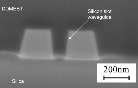
A vapour-deposited organic film covering a silicon waveguide patterned on a silicon-on-insulator substrate.