Lithography
Lithography is a core technology in the manufacturing of semiconductors, enabling the creation of tiny, intricate circuits in chips and microprocessors. With continuous advancements in extreme ultraviolet (EUV) lithography, the industry is pushing the boundaries of smaller nodes and higher performance chips. This innovation has been critical in the development of 5G, AI, and automotive electronics. As demand for smaller, faster, and more energy-efficient devices grows, lithography remains a key enabler of next-generation electronics manufacturing. The global race for leading-edge process nodes continues, positioning lithography as a critical technology in the electronics supply chain.
Posted on 10th October 2025 | Modified on 13th October 2025
AI, Manufacturing, Military/Aerospace Electronics, News, Process R&D
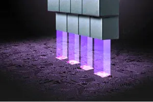
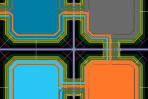
A hyper-beam array lithography system has been introduced to the US, based on architecture pioneered in Europe. The lithography tool operates with 65,000 independently controlled parallel beams which delivers capabilities at a scale no electron beam technology can match, said the company. Installed at Northrup Grumann, it addresses the holy grail of chip design, said founder and CEO, Lex Keen. ...
Posted on 30th September 2025 | Modified on 2nd October 2025
Digital Integrated Circuits, Displays
Aiming at lithography, Texas Instruments has created a digital micromirror device (DLP) with 8.9 million pixels that update at 110Gpixel/s. “Mask-less digital lithography machines – which project light materials without a photomask or stencil – are becoming increasingly popular for the manufacturing advanced packaging [that] combines multiple chips and technologies into a single package,” according to the company. DLP991UUV, as ...
Posted on 22nd September 2025 | Modified on 22nd September 2025
Research
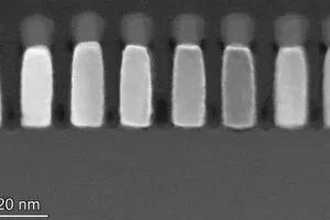
Belgian research lab Imec has revealed advances single-print high numerical aperture EUV lithography at the ‘SPIE Photomask Technology + EUV Lithography’ conference in Monterey California: Line structures at 20nm pitch with 13nm tip-to-tip CD (critical dimension) – relevant for damascene metallisation Electrical test on 20nm pitch ruthenium lines obtained using direct metal etch From the left: 20nm pitch line structures ...
Posted on 1st October 2024 | Modified on 1st October 2024
News
Semiconductor photomask supplier, Toppan Photomask will change its name to Tekscend Photomask, from 01 November. The new name is a combination of technology and ascend, said the company’s press release, a sign, it says, of its commitment to develop its technical capabilities and to grow as a photomask provider. The company’s new logo depicts a photomask over a semiconductor wafer. ...
Posted on 6th May 2021 | Modified on 7th May 2021
Business, Uncategorised
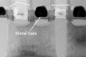
IBM has announced development of a semiconductor process using a 2nm gate all-around (GAA) transistor which delivers a transistor density of 333 million transistor/mm2. The process, compared to 7nm, improves performance by 45% at the same power, or 75% energy at the same performance, compared to modern 7nm processors. The three-stack GAA transistor has a cell height of 75nm, a ...
Posted on 25th March 2021 | Modified on 20th June 2025
EDA and IP, Manufacturing
X-Fab Silicon Foundries has added a photodiode-specific process core module to its XS018 180nm CMOS sensor process – previously XS018 had been focused on the fabrication of multi-pixel CMOS image sensors. Through the new module, customers get access to six different photodiode options covering wavelengths from ultra-violet through to near-infra-red. Amongst the photodiodes, 40% quantum efficiency is available in the UVA ...
Posted on 7th May 2020 | Modified on 7th May 2020
Research
Chemnitz University of Technology has reported a steerable jet-powered micro-submarine, built using wafer processing techniques. Curious, Electronic Weekly got in touch with the team to find out more. A note on the diagram (right) – this is the best diagram of the basic structure we can get our hands on, although it is of a future concept rather than the ...
Posted on 25th May 2018 | Modified on 29th May 2018
Research
A process flow for six-transistor (6T) SRAM suitable for 5nm chips has been created by Imec.
Posted on 8th November 2017 | Modified on 8th November 2017
Design
A company called 3devised is working on a high-resolution 3D printer that occupies only 155 x 155 x 290mm but can print 85.4 x 48 x 130mm. Called Pluto, it uses stereolithography, with a liquid print medium which polymerises to a solid under the influence of ultra-violet light. In this case, the light comes from a 5W UV led, steered by ...
Posted on 14th January 2016 | Modified on 18th June 2019
Research
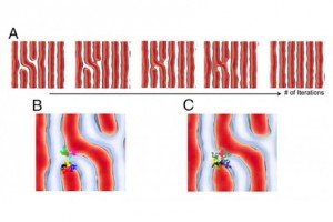
Self-assembling polymers could boost the resolution of lithography, according to modelling at the University of Chicago and US Argonne National Laboratory. Belgian research lab IMEC is testing the theory. Block copolymers will self-assemble when coated onto a patterned surface. The trick is to pre-pattern the surface well enough so that the lowest energy state for the polymer is the desired ...
 Electronics Weekly