 Electronics Weekly
58 partners, including large companies, SMEs, research institutes, universities and industry associations, will spend three yeas on a project named Genesis, aligned with the European Green Deal and European Chips Act, and coordinated by French research lab CEA-Leti.
“Genesis is designed to address the complex challenges of building a truly sustainable semiconductor ecosystem,” said and Leti sustainable electronics program director Laurent Pain. “Its structure reflects both the urgency and the opportunity of Europe’s green transition, powered by the expertise and collaboration of its partners.”
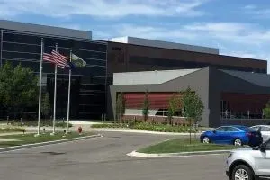
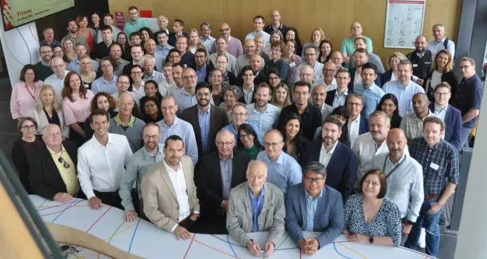 Genesis’ genesis – partner representatives kick off the programme
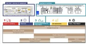
It has four pillars:
- Monitoring and sensing: Real-time emissions tracking, traceability and process feed-back systems
- New materials: PFAS-free chemistries and low-GWP alternatives
- Waste minimisation: Recycling and reusing solvent, gasses and slurries, and finding sustainable replacements
- Critical raw materials mitigation: Strategies to reduce dependency on these, and to strengthen resource security
Alongside these pillars, an overall framework will be established to deploying sensor-integrated abatement systems to reduce PFAS and GHG emissions. “It also aims to position Europe as a leader in green semiconductor innovation by aligning supply-chain practices with environmental regulations,” according to Leti.
Around 45 necessary innovation have so far been identified, said project manger Pain.
Fraunhofer Institute for Photonic Microsystems is a partner, assigned to minimise chemical waste, including tackling the PFSAs (perfluorinated and polyfluorinated alkyls) mentioned above, as well as focussing on emissions of persistent greenhouse gasses.
“We are concentrating on replacing and reducing the emission of climate-damaging gases such as SF6 or NF3. These gases are 10,000 times more harmful than CO2, but are needed in the semiconductor industry,” said Fraunhofer IPMS project lead Erik Schumann. “We are also working to reduce the waste produced during chemical mechanical polishing.”
European Commission funding for Genesis is being channelled through Chips Joint Undertaking (Chips JU) – a public-private partnership created to foster collaboration between the EU, its member states and the semiconductor private sector.
“As chips become the backbone of everything from AI to energy systems, their environmental footprint is rapidly growing,” said Chips JU head of programmes Anton Chichkov. “The launch of the Genesis project marks a critical step toward aligning Europe’s semiconductor ambitions with its climate commitments. Through this initiative, Europe is not only investing in cleaner technologies, it is positioning itself as a global leader in green semiconductor manufacturing.”
 Alongside EC/Chips JU funds are also coming from participating EU member states and SERI, the Swiss State Secretariat for Education, Research and Innovation.
