Electronics Weekly
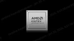
The XC2KU040P and XC2KU050P FPGAs are likely to have six 32-bit hard LPDDR memory controllers, operating at 4,266Mbps. The FPGAs will also have high-speed transceivers and frame-accurate transport for professional broadcast and remote production applications.
They will be suitable for high-throughput test and measurement, advanced imaging and real-time control in machine vision, industrial automation, medical imaging and robotic systems, said AMD.
Equipped with integrated LPDD4X/5/5X controllers with high DDR bandwidth, the mid-range FPGAs will have a five-fold increase in memory bandwidth compared to the previous generation and up to double the channel density per PCIe interface, for high throughput and low latency operation. They will deliver up to 80% higher embedded RAM and twice the DSP density and higher LPDDR memory bandwidth than competing FPGAs, claimed AMD.
Other features are scalable, high-speed I/O and deterministic fabric behaviour for faster on-device processing and adaptable pipelines for responsive real-time behaviour, said the company. Security features include authenticated device operation, bitstream encryption, anti-cloning protection, secure key management and CNSA 2.0 grade cryptography.
Pre-production XC2KU050P FPGA silicon will begin sampling in Q4. AMD will also release a Kintex UltraScale+ Gen 2 evaluation kit based on the FPGA at the same time. Production of the XC2KU050P FPGA is scheduled for the first half of 2027.
AMD said that the Kintex UltraScale+ Gen 2 series will be available at least until 2045.