Electronics Weekly
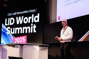
Jean-René Lèquepeys presenting at Leti Days 2025. Credit: CEA-Leti
Artificial intelligence (AI) is now central to computing, but its appetite for power is growing unsustainably. As large language models, autonomous systems and edge applications proliferate, AI is demanding more from hardware than any previous class of workloads. Unless the trajectory changes, AI systems will soon become one of the largest consumers of electricity on the planet.
“We are reaching planetary limits,” warns Jean-René Lèquepeys, CTO of CEA-Leti, in a keynote at Leti Innovation Days (LID) 2025 in Grenoble. “The energy cost of moving and processing data is exploding. We need new paradigms – not just incremental improvements.”
Leti is spearheading a Europe-wide effort to radically reduce energy use in AI hardware. The initiative, called RESOLVE (Reducing Energy Consumption for Sovereignty and Leadership in Value-Added European Products), spans 15 interrelated research tracks and includes dozens of industrial and academic partners. Its goal: a 1,000-times improvement in energy efficiency by 2032.
The energy demands of AI are felt at both ends of the value chain. Training large foundation models requires tens of MWhrs, while inference is becoming increasingly demanding as models move into production and edge use cases. Generative models, in particular, are being integrated into daily workflows across industries, multiplying the number of inferences and spiking power consumption even at idle.
The push to bring inference closer to users, where latency is lower and data can remain local, has compounded hardware design challenges. “Today, we expect AI to run on everything from smartphones to autonomous sensors,” Lèquepeys told Electronics Weekly. “That’s a very different problem than training in the cloud.”
Edge AI requires energy-efficient processing that can operate within tight power budgets, often without active cooling or consistent connectivity. Yet as the models grow in complexity the traditional separation between memory and compute is becoming the primary bottleneck.
That bottleneck is known as the memory wall – the growing latency and energy cost of moving data between memory and processing units. “The cost of computation is no longer the limiting factor,” said Lèquepeys. “It’s the cost of data movement.”
The memory wall is especially problematic in AI, where neural networks may need to access and update millions – or billions – of parameters in real time. For inference to work efficiently at the edge, memory needs to be both fast and physically close to the compute logic.
A hardware revolution in the making
CEA-Leti is addressing the memory wall from multiple angles. One involves exploring new materials for non-volatile memory, such as resistive RAM, magnetic RAM, and ferroelectric RAM (FeRAM). These technologies promise faster access times, lower write energies and better endurance than traditional flash.
Leti has shown in recent demonstrations that FeRAM can reduce programming power by a factor of 20,000 compared to flash. Its endurance exceeds 10 million write cycles, making it viable for edge workloads.
The institute is also pursuing 3D integration techniques, especially 3D sequential stacking, where additional layers of transistors are fabricated directly on top of existing ones. This approach brings memory and logic physically closer, reducing the time and energy needed to shuttle data between them.
“Unlike conventional stacking, where dies are packaged together, 3D sequential allows us to stack transistors and interconnects with nanometre precision,” says Lèquepeys. “That’s a game-changer for density and performance.”
In one prototype Leti built a chip with two full layers of transistors and nine layers of metal interconnect, delivering compute power equivalent to 10 laptops on a chip smaller than a postage stamp. The energy-efficiency improved by a factor of 10 over traditional architectures.
To further reduce power and latency in complex systems Leti is developing new packaging and interconnect strategies. These include advanced chiplet-based designs, where small function-specific dies are interconnected on an interposer and co-packaged optics, where data moves between chips via photons instead of electrons.
“We’ve demonstrated on-chip optical networks using both silicon photonics and gallium nitride micro-LEDs,” says Lèquepeys. “The latter offers ultra-low latency and up to 10-times better energy efficiency.”
Optical interconnects could become especially important for datacentres, where power consumption is expected to grow dramatically.
While chiplets offer flexibility and better yields, Lèquepeys is frank about the challenges. “We’ve been exploring chiplets for 15 to 20 years. Technologically, they work. But to scale, especially for sectors like automotive, we need open standards and a shared library of functions – like Arm did for CPUs.”
Leti is also focused on improving chip manufacturing, using AI to optimise wafer lots, predict defects and manage thermal budgets in advanced 3D integration flows. AI models and digital twins help reduce trial-and-error, enabling faster development and lower costs.
AI is embedded in design too. Leti’s open-source N2D2 platform allows developers to explore neural networks under hardware constraints, balancing memory size, latency and energy efficiency. In perception tasks N2D2-optimised models have delivered 10-times energy savings compared to conventional approaches, according to Lèquepeys.
Collaborating for scalable, sustainable AI
While RESOLVE is a European project, Genesis is a related project co-ordinated by Leti. It involves 58 partners across 12 countries and aims to decarbonise chip manufacturing. Its goals include eliminating PFAS chemicals, reducing water use and improving recycling processes.
“Only 15% of electronic waste is recycled today,” Lèquepeys says. “We’re still extracting more raw materials than at any time in human history. That’s not sustainable.”
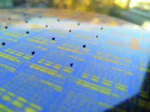
GaN dies stacked on 200mm Si wafer. Credit: CEA-Leti
Leti is embedding sustainability into design from the start. Its fabs are reusing water and applying low-emission processes. Lifecycle analysis is being used earlier in the design process to reduce environmental impact from concept through disposal.
Schneider Electric, Soitec and FMC are already piloting Leti’s technologies in power electronics and digital manufacturing.
At the policy level a second European Chips Act is gaining traction. With support from nine EU member states, the European Commission and industrial alliances, it could provide the funding and infrastructure needed to accelerate adoption.
As LID 2025 concluded Lèquepeys offered a final reflection. The semiconductor industry, he said, stands at a crossroads – between declinism, which accepts stagnation, and sobriety, which seeks responsible innovation.
“AI can solve enormous problems but only if we solve the energy problem first,” he says. “We can’t keep scaling performance without thinking about what it costs the planet. The solution is not to slow down – but to move forward smarter, cleaner, and together.”