Electronics Weekly
By engineering the device structure of ferroelectric memory and introducing a nanogate-induced electric field concentration effect, the researchers developed a ferroelectric transistor capable of operating at a voltage of 0.6V.
The device achieves an energy consumption of 0.45 fJ/μm and reduces the physical gate length to the ultimate 1nn limit.
Polarisation switching and data erase/write operations typically require voltages above 1.5V. Although already more efficient than Flash memory, traditional designs cannot theoretically reduce operating voltages below 0.7V—preventing compatibility with mainstream logic voltage levels.
Thus, how to achieve sub-0.7V ultralow-voltage memory operation has become a critical challenge for breaking through memory bottlenecks and enhancing AI chip performance.
By aggressively scaling the gate electrode to the nanometer limit, the researchers harnessed the tip-induced electric field concentration effect of the nanogate.
This design creates a highly localized and intensified electric field region within the ferroelectric layer, significantly amplifying local field strength and dramatically lowering the voltage required for polarization switching. The approach surpasses the coercive voltage limits of conventional planar ferroelectrics and overturns the long-standing trade-off between low operating voltage and high coercive electric field.
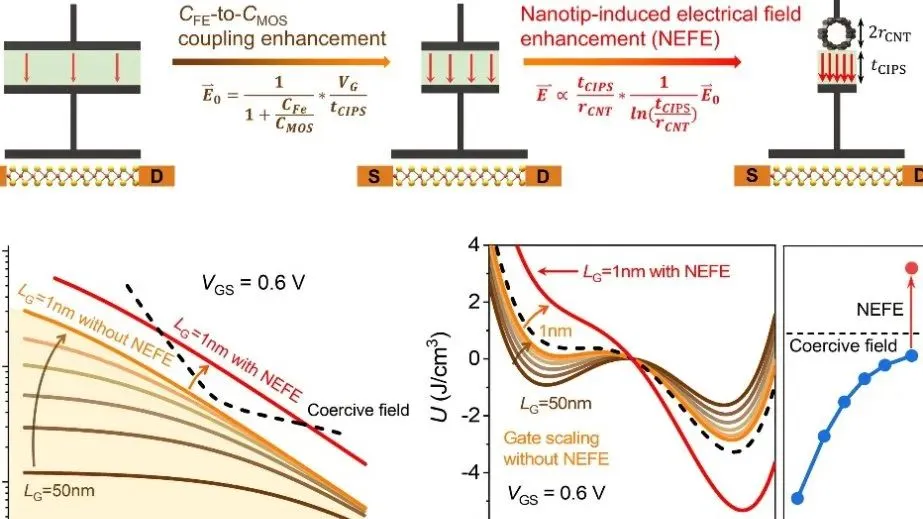
Notably, the study reveals an anomalous scaling advantage in ferroelectric transistors: as the physical gate length shrinks to the 1nm limit, electric field convergence and enhancement become significantly stronger.
The extremely small gate dimension effectively improves ferroelectric memory characteristics, underscoring the substantial potential of ferroelectric memory technologies in future sub-nanometer node chips.