Electronics Weekly
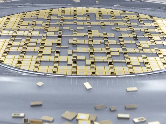
Currently sampling to potential customers, the parts will all be variants of the new part number ‘MLX91299’, and be delivered as a bare die ready for top-side wire-bonding alongside mosfet and diode die inside the power module. The back metallisation is compatible with both sintering and soldering.
Designed for dc-links operating at up to 1,000Vdc, with peaks up to 1,200V, the silicon snubber will have breakdown ratings above 1,500V.
They will “maintain constant capacitance for voltages above 150V and exhibit leakage current around 10nA”, according to the company. “Various R and C combinations are available, such as 4.3nF at 1.45Ω or 1.1nF at 5.23Ω.”
Exactly which variants will be produced has not yet been decided.
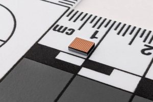
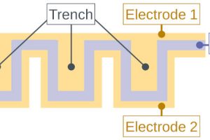
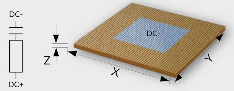
 The size limits are: between 1.5 and 5mm across (X and Y in top diagram), and up to 640μm thick (Z). Capacitance from 200pF to 5.8nF is possible, and resistance from 1Ω to 35Ω. The target for operation is across -40 to +150°C ambients, with 175°C peak device temperature.
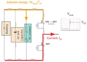
As well as functioning as a dc link snubber, output snubbing in parallel with a mosfet is also envisaged.
“Operating at fast switching speeds and elevated voltages, SiC devices are inherently susceptible to voltage transients, high-frequency oscillations and parasitic effects,” said Melexis. “Integrating an RC snubber mitigates these effects, and early measurements from Melexis show the RC snubber can reduce switching losses by up to 50%.” – This 50% figure was from 91mJ with no snubber, to 39mJ with a silicon snubber.
Texas Instruments clearly sets out seven steps to RC snubber design in an app note