Electronics Weekly
 Designers looking to implement artificial intelligence (AI) algorithms on inference processors at the edge are under constant pressure to lower power consumption and development time, even as processing demands increase. FPGAs offer a combination of speed and power efficiency for implementing the neural network (NN) inference engines required for edge AI.
Why use AI at the edge?
Edge computing brings a number of benefits to IoT applications in segments as varied as industrial automation, security systems and smart homes. In an industrial IoT application targeting the factory floor, edge computing can dramatically improve response time in process control loops by eliminating round trip delays to cloud-based applications. Similarly, an edge-based security system or smart home door lock can continue to function even when the connection to the cloud is lost accidentally or intentionally.
The rapid acceptance and increased demand for machine learning (ML) inference models dramatically amplifies the importance of edge computing. For developers, local processing of inference models helps to reduce response latency and the costs of cloud resources required for cloud-based inference. For users, the use of local inference models adds confidence that products will continue to function despite occasional loss of internet connectivity or changes in the product vendor’s cloud-based offerings.
Developing an NN inference model for vision-based object detection begins with model training, typically performed on an ML framework such as TensorFlow using publicly available labelled images or custom labelled images. The processing demands mean model training is typically performed with GPUs in the cloud or another high-performance computing platform. When training is complete, the model is converted to an inference model able to run on edge or fog computing resources and deliver the inference results as a set of object class probabilities (Figure 1).
Using FPGAs to accelerate NN maths
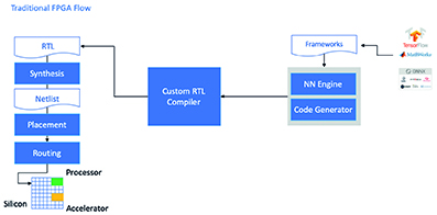 FPGAs are sometimes bypassed due to a traditional development flow that can be daunting to developers without extensive FPGA experience. To create an effective FPGA implementation of an NN model generated by an NN framework, the developer needs to understand the nuances of converting the model into register transfer language, synthesising the design and working through the final place and route physical design stage to produce an optimised implementation (Figure 2).
Microchip Technology’s PolarFire FPGAs, specialised software and associated intellectual property (IP) make high performance, low power inference at the edge broadly available to developers without FPGA experience.
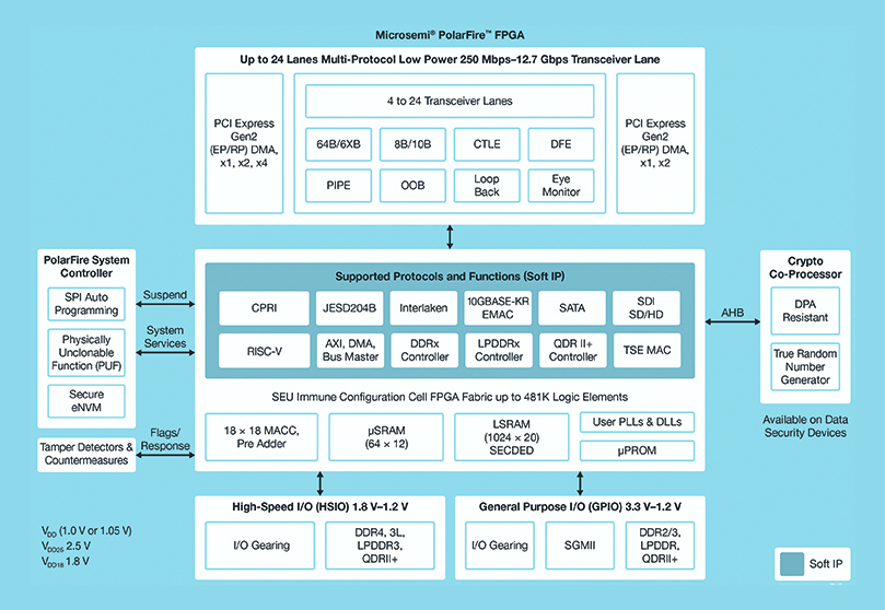 These FPGAs are designed to maximise flexibility and performance while minimising power consumption. They feature a deep FPGA fabric able to support advanced functionality using soft IP cores, including RISC-V processors, advanced memory controllers and other standard interface subsystems (Figure 3).
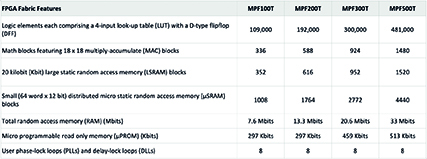
The PolarFire FPGA fabric provides a set of logic elements and specialised blocks, supported in a range of capacities by different members of the PolarFire family (see Table 1).
The PolarFire architecture accelerates mathematical operations and helps relieve the kind of memory congestion encountered when implementing inference models on general purpose architectures, such as small distributed memories for storing intermediate results created during NN algorithm execution. An NN model’s weights and bias values can be stored in a 16-deep by 18-bit co-efficient ROM built from logic elements located near the math block.
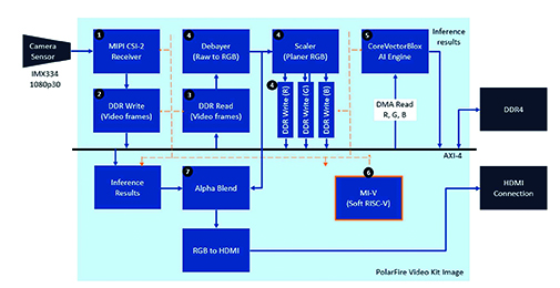
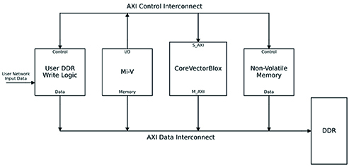 A complete NN processing system would combine a CoreVectorBlox IP block, memory, memory controller and a host processor, such as the RISC-V (Mi-V) software processor core (Figure 4).
In a video system implementation, the host processor would load the firmware and network binary large objects (BLOBs) from system flash memory and copy them into double data rate (DDR) RAM for use by the CoreVectorBlox block. As video frames arrive, the host processor writes them into DDR RAM and signals the CoreVectorBlox block to begin processing the image. After it runs the inference model defined in the network BLOB, the CoreVectorBlox block writes the results back into DDR RAM for use by the target application.
Instead of dealing with the details of the traditional FPGA flow, NN model developers work with their NN frameworks as usual and load the resulting model into Microchip’s VectorBlox Accelerator software development kit (SDK). This generates the required set of files including those needed for the normal FPGA development flow and the firmware and network BLOB files.
The VectorBlox Accelerator SDK flow overlays the NN design onto the NN engine implemented in the FPGA, enabling different NNs to run on the same FPGA design without the need to redo the FPGA design synthesis flow.
 The SDK melds the Libero FPGA design suite with a set of capabilities for NN inference model development. It also provides an NN simulator that lets developers use the same BLOB files to evaluate their model prior to their use in the FPGA hardware implementation.
The SDK supports models in the Open Neural Network Exchange format as well as models from a number of frameworks including TensorFlow, Caffe, Chainer, PyTorch and MXNET. Supported convolutional NN architectures include MNIST, MobileNet versions, ResNet-50, Tiny Yolo V2 and Tiny Yolo V3. Microchip is working to expand support to include networks in the open-source OpenVINO toolkit open model zoo of pre-trained models, including Yolo V3, Yolo V4, RetinaNet and SSD-MobileNet.
Video and imaging kit
To help developers move quickly into smart embedded vision application development, Microchip provides a comprehensive sample application designed to run on the company’s MPF300-Video-Kit PolarFire FPGA video and imaging kit and reference design.
The kit comes with a complete Libero design project used to generate the firmware and network BLOB files. After programming the BLOB files into on-board flash memory, developers click on the run button in Libero to start the demonstration (Figure 5).
 The demonstration supports acceleration of Tiny Yolo V3 and MobileNet V2 models, but developers can run other SDK supported models using the methods described earlier.
AI algorithms, such as NN models, typically impose compute-intensive workloads that require more robust computing resources than available with general purpose processors. Using specialised IP and software, developers without FPGA experience can implement inference-based designs better able to meet performance and power, as well as design schedule requirements.