Electronics Weekly
Achieving a net data rate of 400Gb/s per lane and optimized for compactness, low latency, and high energy efficiency, imec’s modulator establishes the foundation for next-generation optical IM/DD (intensity modulation with direct detection) links that interconnect datacentre racks and blade servers in a simple and cost-effective way.
The technology will be key to meeting the demands of AI applications that rely on ever-faster, more efficient machine learning training.
AI applications – and the machine learning training that drives them – require compute architectures capable of exchanging massive volumes of data with near-instant responsiveness. Meeting this challenge calls for short-reach, scale-up interconnects between data center racks and blade servers, delivering minimal latency and bit rates of 400Gb/s per lane (now widely regarded as the benchmark for future-ready deployments). Optical IM/DD links powered by electro-absorption modulators (EAMs) are emerging as a key enabler.
“Developing the right modulators to support these optical IM/DD links has been a major research focus, as commonly-used technology options all have drawbacks,” says Cedric Bruynsteen, a researcher at IDLab – an imec research group at Ghent University (Belgium). “Thin-film lithium niobate Mach-Zehnder modulators (MZMs), for instance, offer excellent linearity, low optical loss, and very high bandwidth, but their large footprint and contamination challenges hinder wafer-scale integration with advanced CMOS logic, challenging their use for future co-packaged optics and optical I/O. Micro-ring modulators, on the other hand, provide high integration density but require substantial stabilization control circuitry, which limits their energy efficiency.”
It combines ultrahigh bandwidth, 400Gb/s per lane IM/DD transmission, and wafer-scale manufacturability in a C-band device – for the next generation of optical interconnects.
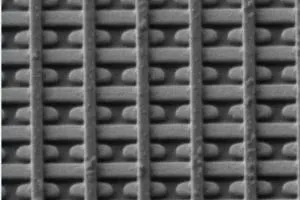
“Our C-band GeSi EAM addresses these challenges head-on. By exploiting the Franz-Keldysh effect, it achieves compactness, high speed, and low power consumption,” adds Bruynsteen, “and thanks to its GeSi foundation, it integrates seamlessly on our 300mm silicon photonics platform – enabling mass-market manufacturability.”
Imec’s achievement combines two world’s firsts: the first demonstration of a beyond-110GHz GeSi EAM operating in the C-band, and the first realization of a net 400Gb/s per-lane transmission with any silicon-based EAM.
It is a breakthrough that builds on more than a decade of progress at both the device integration and system level. On the device integration side, imec researchers optimized footprint dimensions, doping schemes and epitaxial growth processes. On the system side, they developed a robust transmission setup that showcased the EAM’s capability for a net 400Gb/s per-lane data transmission, operating in a PAM-4 IM/DD link.
“These results clearly illustrate the potential of our GeSi EAM to enable next-generation, scale-up optical interconnects. Interestingly, however, the modulator itself was never the limiting factor in our bandwidth experiments – it was the measurement equipment that capped us at 110GHz. Hence, with access to higher-frequency measurement tools, the next step is to uncover the device’s true bandwidth limits and evaluate its performance under higher temperatures representative of data center conditions,” concluded Bruynsteen.
Imec is making the GeSi EAM available to partners, enabling them to explore its potential for scale-up networks inside AI training clusters.
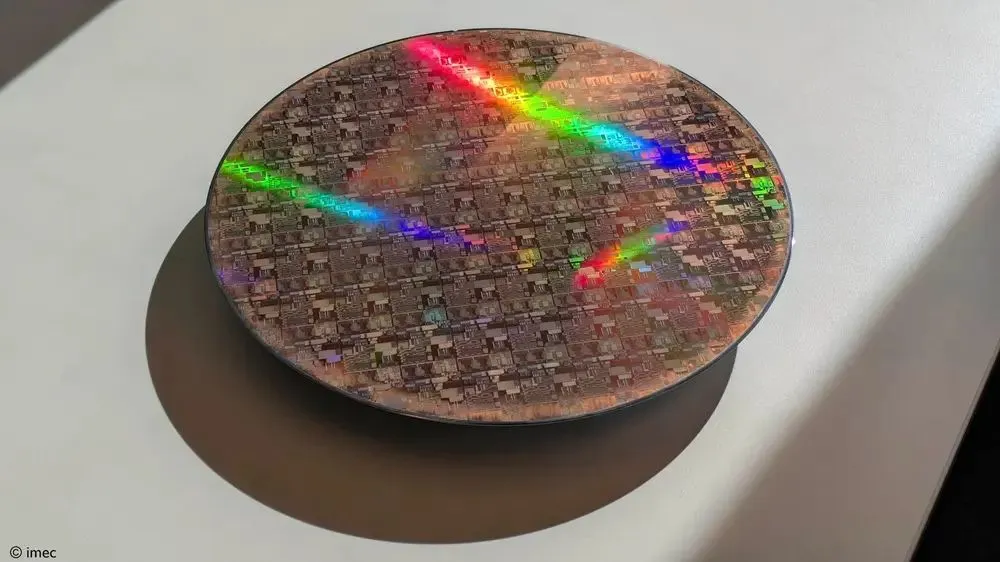
For more: 300mm silicon photonics platform and prototyping services