Home » News » Research » Device R&D (page 2)

Device R&D

Glasgow’s CST samples lasers for 10G optical networks

DFB20laser20production20at20CST20Global-300x200.jpg

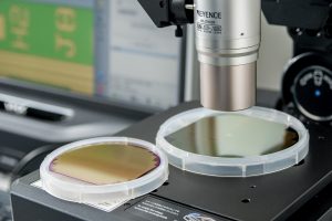
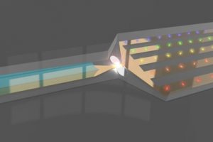
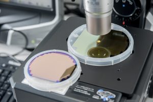
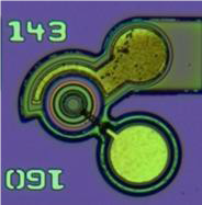
CST Global, the Glasgow semiconductor laser manufacturer, says it is sampling its 1270nm, 2.5Gbit/s asymmetric and 10Gbit/s symmetric, DFB lasers for 10G PON (passive optical network) applications. The firm is currently beta sampling its asymmetric 2.5Gbit/s lasers and alpha sampling its symmetric, 10Gbit/s lasers. The asymmetric beta samples, which are undergoing ITU-GR468 reliability testing, are available for customer trials in ...

French technology improves microdisplays

PWbooth1-300x200.jpg

Next week at SPIE Photonics West in San Francisco, French research centre Leti will demonstrate a new curving technology for optical components that widens field of view and compensates for optical aberrations. Called Pixcurve, it is a proof of concept for optical components such as microdisplays, visible imagers and cooled infrared sensors used in mobile phones, telescopes, medical-imaging tools, IR ...

Cardiff laser conference hears about 50Gbit/s data rates

850nm20VCSEL2c20CST20Global.png

Project engineer, Iain Eddie from CST Global, the Scotland-based III-V opto-electronic, semiconductor foundry, will present a paper on high-speed 850nm VCSELs (Vertical Cavity Surface Emitting Lasers) at the VCSEL Day in Cardiff this week (8th and 9th June). These lasers are expected to be used for data transmission rates of 50Gbit/s. VCSELs have the benefit of offering a high bandwidth ...