Posted on 20th September 2017 | Modified on 20th September 2017
News, Process R&D
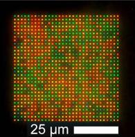
Scientists at the University of Glasgow say they have developed a new form of high-resolution ‘printing’ which could have wide-ranging applications in data storage, anti-counterfeiting measures, and digital imaging. The research, published in the journal Advanced Functional Materials, describes the development of nano-scale plasmonic colour filters that display different colours depending on the orientation of the light which hits it. ...
Posted on 29th June 2017 | Modified on 29th June 2017
News, Process R&D, Research
Leti, the French semiconductor research institute, teams with Fraunhofer’s microelectronics group to extend next generation CMOS technologies for the IoT
Posted on 24th February 2017 | Modified on 27th February 2017
Business, Process R&D
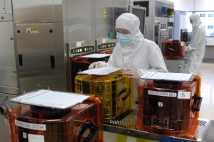
Imec has its funding from the Flanders government increased to $108 million a year for the next five years.
Posted on 8th December 2016 | Modified on 12th June 2025
News, Process R&D
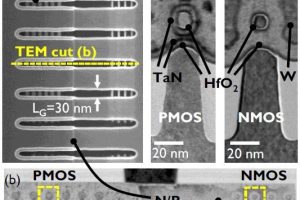
Imec has achieved the CMOS integration of vertically stacked gate-all-around (GAA) silicon nanowire MOSFETs. Key in the integration scheme is a dual-work-function metal gate enabling matched threshold voltages for the n- and p-type devices. Also, the impact of the new architecture on intrinsic ESD performance was studied, and an ESD protection diode is proposed. These breakthrough results advance the development ...
Posted on 8th June 2016 | Modified on 8th June 2016
Market Research, News, Process R&D
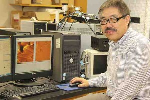
Imec held its Technology Forum in Brussels last month. Electronics Weekly’s components editor David Manners attended the event and his detailed reports on the technology ranging from deep sub-micron semiconductor technology to low power radio, IoT security and solar cells are published in this week’s issue of the magazine. Why is Imec important to the UK electronics industry? It is one of ...
Posted on 27th April 2016 | Modified on 25th June 2025
News, Power, Process R&D
Photovoltaic (PV) module efficiencies of 27% for solar energy generation is the claim of Swedish advanced materials start-up Sol Voltaics using its nanowire technology. Solar power system developers have looked at using nanowires to improve conversion efficiency, but they are notoriously difficult to align due to their high aspect ratios and material characteristics. What Sol Voltaics has done is to ...
Posted on 20th April 2016 | Modified on 17th June 2025
Device R&D, News, Process R&D
Researchers at the University of Georgia and at Ben-Gurion University in Israel claim to have demonstrated how nanoscale electronic components can be made from single DNA molecules. According to the study’s lead author, Bingqian Xu, an associate professor in the UGA College of Engineering: “For 50 years, we have been able to place more and more computing power onto smaller ...
Posted on 19th April 2016 | Modified on 19th April 2016
News, Process R&D
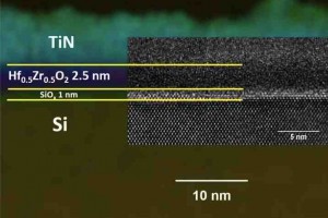
Scientists from the Moscow Institute of Physics and Technology (MIPT) have succeeded in growing ultra-thin (2.5-nanometre) ferroelectric films based on hafnium oxide that could potentially be used to develop non-volatile memory elements called ferroelectric tunnel junctions. As demand for data storage increases researchers are trying to develop faster and more compact storage devices. The ideal would be a “universal” memory ...
Posted on 15th April 2016 | Modified on 18th April 2016
News, Process R&D
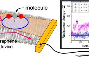
Researchers at the University of Southampton claim to have developed a graphene-based sensor that can detect harmful air pollution in the home with very low power consumption. The sensor, which is the result of a collaboration with the Japan Advanced Institute of Science and Technology (JAIST), detects individual CO2 molecules and volatile organic compound (VOC) gas molecules found in buildings ...
Posted on 12th April 2016 | Modified on 12th April 2016
Communications, News, Process R&D
A 3D chip technology, which stacks active layers of transistors without the need for through-silicon vias (TSVs) has been developed by Leti and is the focus of a collaboration with Qualcomm. Dubbed CoolCube, the French research centre has developed a device scale-stacking technology for complex system-on-chips such as mobile processors which is why Qualcomm is collaborating with Leti. The technology ...
 Electronics Weekly