Electronics Weekly
 Working with lithography equipment supplier Mapper Lithography, Leti says it has perfected a way to generate a non-falsifiable code using a new chip design that leverages direct multi-beam writing in a process that fits in a conventional CMOS flow with an extra level of lithography and without photomasks.
Leti and Mapper presented a paper on the work called: “Process development of a maskless N40 via level for security application with multi-beam lithography”, at last month’s SPIE Advanced Lithography 2018 in California.
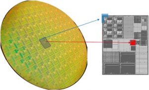
The paper demonstrates a via patterning integration that is compliant with standard CMOS 40nm process flow.
“Standard optical exposure tools – optical scanners using masks – repeat the identical design on the entire silicon wafer, and cannot fabricate individualised chips,” said Leti’s Isabelle Servin, the lead author of the paper.
“Leti applied its deep multi-beam lithography knowhow and Mapper‘s unique maskless fabrication tools to achieve this differentiating, cyber-security chip.”
The maskless lithography system is based on massively parallel electron-beam writing capability.