Electronics Weekly
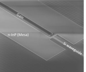
Microscopy view of the III-V/Si DFB laser after the IIIV patterning steps
Leti says it has integrated hybrid III-V silicon lasers on 200mm wafers using standard CMOS process flow.
“This shows the way to transitioning away from 100mm wafers and a process based on bulk III-V technology that requires contacts with noble metals and lift-off based patterning,” said Leti.
Using a CMOS process for silicon photonics lowers fabrication costs, and provides access to mature and large-scale facilities, which enables packaging compatibility with CMOS driving circuits.
Being able to fabricate an integrated light source is important for silicon-photonic technologies.
Bertrand Szelag, a co-author of the paper, writes:
“This project showed that a laser can be integrated on a mature silicon-photonic platform with a modular approach that does not compromise baseline process performances. We demonstrated that the entire process can be done in a standard CMOS fabrication line with conventional process and materials, and that it is possible to integrate all the photonic building blocks at large scale.”
The laser can be integrated on a mature silicon photonic platform with a modular approach that, according to the researchers, does not compromise the baseline process performance.
Next steps include integrating the laser with active silicon-photonic devices, e.g. a modulator and photodiode with several interconnect metal levels in a planarised backend. Finally, III-V die bonding will replace III-V wafer bonding in order to process lasers on the entire silicon wafer.
The project, carried out in the framework of the IRT Nanoelec program, which is headed by Leti, demonstrated that the hybrid device’s performance is comparable to the reference device fabricated with the current process on 100mm wafers.
The results were reported Dec. 5 at IEDM 2017 in a paper titled “Hybrid III-V/Si DFB Laser Integration on a 200mm Fully CMOS-compatible Silicon Photonics Platform”.