 Electronics Weekly
Soitec says FD-SOI (fully-depleted silicon-on-insulator) has the potential to become an important high volume next-generation semiconductor process technology. The French FD-SOI semiconductor technology supplier was speaking following the announcement of an FD-SOI fab deal between Samsung and STMicroelectronics. It said the supply chain for the technology is in place. “It also represents a tipping point for FD-SOI industry deployment,” said Soitec. Samsung is licensing ...
Process R&D
Manchester deal puts graphene on road to commercial market
A company quoted on London’s AIM stock market company has bought major stake in a spin-out company developing graphene semiconductor products based on technology pioneered at the University of Manchester. This is a big step in the commercialisation of the university’s Nobel Prize-winning grapheme research. Versarien has acquired a controlled 85% equity stake in 2-DTech, which is a graphene company ...
SureCore tests first ‘low-power’ SRAM chip
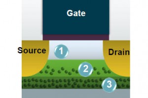
SureCore has said that the first tests of its low power SRAM design confirm its simulations and “deliver in excess of 50% power savings over other SRAM technologies”. The UK-based embedded memory process developer taped out its low power SRAM IP demonstrator chip in October on STMicroelectronics’ 28nm Fully Depleted Silicon-on-Insulator (FD-SOI) process. The device was used to validate the benefits of the start-up’s patented ...
Imec: 30 years of world beating chip research
Belgium-based nanotechnology research centre Imec is celebrating its 30th anniversary. Founded in 1984 as a non-profit organisation, Imec has grown to be a multi-disciplinary R&D centre in the fields of semiconductor chips and systems, electronics for life sciences, photovoltaics, image sensors and flexible electronics and displays. Imec has played an important role in advancing immersion lithography, EUV, double patterning for ...
Qualcomm assesses Leti’s 3D chip technology, it is not TSV
Qualcomm Technologies has signed a technology agreement with CEA-Leti to assess the implementation of the French research centre’s sequential 3D technology. In recent years, Leti has been actively working on a new 3D integration technology process called sequential 3D integration that enables the stacking of active layers of transistors in the third dimension. This is not through silicon via (TSV) ...
Printable electronics start-up produces 6V display driver

An Oslo-based start-up developing printed electronics circuits has demonstrated a low-voltage display driver which operates at 6V and is capable of driving electrochromic displays. The company, Thin Film Electronics ASA, came to prominence when it commercialised printed rewritable memory. It is now creating other printable electronic circuits using complementary organic transistor logic. Thinfilm’s transistor technology, developed together with Polyera and others, has a voltage operating range from 3 to 20V. ...
Fujitsu turns to SuVolta to halve Cortex-A0 power consumption
Deeply depleted channel (DDC) transistors have enabled Fujitsu to halve the power consumption of a 65nm ARM Cortex-M0 core. The technology, licenced from SuVolta, reduces process variations by removing dopant atoms from the channel, without resorting to finfets or SoI wafers. Without dopant-derived transistor threshold variations, all the devices on a particular chip are better matched in leakage and speed ...
Diamond-like thin film devices could be used as medical sensors
Finnish coating technology specialist Picodeon has developed a technique for depositing very hard diamond-like films onto a range of different substrates using its patented ultra-short pulsed laser deposition (US PLD) technology. The coatings create surfaces with hardness greater than 40Gpa, and with a low coefficient of friction. This will have benefits in applications such as machine tooling components and worn components ...
7 countries, 19 partners, 500 engineers, to spend $360m on FD-SOI
STMicroelectronics is getting together with Imec to build FD-SOI. A seven nation, 19 partner, $360m, 500-engineer, 3 year, EU-backed project will set up two FD-SOI pilot lines in Crolles and Dresden.
450mm, EUV, struggling
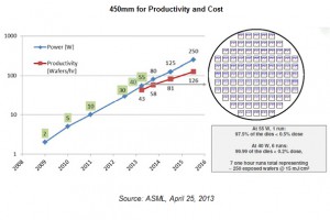
450mm production tools may be in volume production in 2018 and EUV tools may be production-capable in 2016, says ASML.