Posted on 2nd April 2020 | Modified on 2nd April 2020
EDA and IP
The Compact Model Coalition (CMC) has adopted a model from French lab Leti for fully-depleted silicon-on-insulator (FD-SoI) chip simulation. Called L-UTSOI, it was “proven by the industry and its standardisation will ensure long-term access and maintenance in EDA tools for FD-SOI designers”, according to Leti. Available to Coalition members now, it will be implemented in major versions of circuit-simulation software, and its ...
Posted on 27th March 2020 | Modified on 27th March 2020
Business, EDA and IP
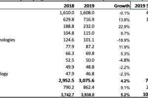
Arm’s revenues declined slightly in 2019 in a market that grew, says IPnest, reflecting similar situations in 2018 and 2017. Arm’s royalty revenue declined by 6-7%, says IPnest, but its licensing revenues – including physical IP – were up 13%. Companies ranked by semiconductor design IP revenue in 2019 (millions of dollars). Source: IPnest (March 2020). ARM once controlled 50% ...
Posted on 24th March 2020 | Modified on 27th March 2020
Business, EDA and IP
Google has come up with a neural net that can do IC design placement in record quick time.
Posted on 18th March 2020 | Modified on 28th March 2025
EDA and IP
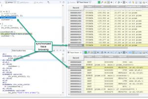
SiFive has announced hardware trace and debug for RISC-V processor IP. Called SiFive Insight, it is intended to, according to the company, “meet customer demand and expectations for the capability to access, observe, and control products deploying SiFive’s RISC-V Core IP portfolio”. “SiFive Insight is the industry’s first integrated RISC-V processor core, trace, and debug IP solution from a single ...
Posted on 16th March 2020 | Modified on 18th June 2025
Business, EDA and IP
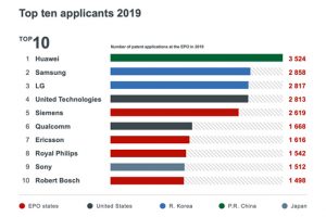
The European Patent Office has released a list of the top patent filers for last year.
Posted on 14th February 2020 | Modified on 20th February 2020
Business, EDA and IP
Moortec, the Plymouth developer of on-chip monitoring and analytics IP, is opening a new design centre in Bristol. It is Moortec’s third design office after Plymouth and Poland. “We’ve a very successful Design office in Poland and our main Head Office in Plymouth – our new additional Design office located in the heart of Bristol will really add to our ...
Posted on 5th February 2020 | Modified on 5th February 2020
Business, EDA and IP, Uncategorised
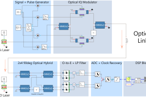
Designers that want to use Infinera InP open foundry services, part of the Infinera Optical Innovation Center, will benefit from a design workflow that starts from a graphical photonic IC design and system simulation environment. The workflow is enabled by VPItoolkit PDK Infinera— a pluggable toolkit extension to VPI Photonic Circuits – which adds by support of the PDK building blocks for the InP-based PIC foundry process ...
Posted on 12th November 2019 | Modified on 23rd June 2025
EDA and IP
Mentor is addressing the functional safety requirements of ICs in autonomous vehicles with an initiative called ‘Tessent Safety Ecosystem’ which links the firm’s own functional safety tools, including those acquired when it bought Austemper, to those from external partners – notably Arm through its Functional Safety Partnership Program. At the same time, it announced a related tool – for adding fast ...
Posted on 29th October 2019 | Modified on 19th June 2025
Automotive Electronics, EDA and IP, Embedded Systems, Products, Software
An Israeli company, Optima Design Automation has introduced two tools for automotive design. The Optima Safety platform consists of Optima-HE and Optima-SE, both based on the company’s Fault Injection Engine (FIE) and designed for fault analysis, targeting safety analysis fault injection for SoC design. The FIE uses parallel simulation and formal verification, rather than fault simulation, and introduces fault list ...
Posted on 28th October 2019 | Modified on 7th May 2025
Business, EDA and IP
Huawei topped the patent application table last year according to WIPO, the World Intellectual Property Organisation. But Tokyo analysts Patent Result says that only 21% of the 5,405 patent applications made by Huawei last year could be regarded as highly innovative, reports the Nikkei. Patent Result asseses patents by a number of criteria including originality, actual technological applications and versatility ...
 Electronics Weekly