Electronics Weekly
 An avalanche photodetector (APD) is able to produce large currents from the input of an extremely low light signal, down to a few photons.
When a photon is absorbed, it excites an electron to the conduction band, leaving a gap in the valence band (called a hole), which behaves in a similar manner to a positively charged particle. These two charge carriers are then separated by an electric field and produce a current. In an APD, the electric field is sufficiently large that the carriers can gain enough energy to excite additional electron-hole pairs, a process known as impact ionisation.
 The freshly ionised electron and hole are then accelerated, leading to a large number of electrons and holes contributing to the current from a single detection event.
The abilities of electrons and holes to cause impact ionisation are quantified by the electron and hole ionisation coefficients α and β. Silicon is a near-ideal APD material, as electrons can readily cause impact ionisation, whereas holes cannot, meaning the α/β ratio is very large and the excess noise due to the stochastic ionisation process is reduced. Silicon’s indirect band gap, however, means that thick layers are required to absorb photons, and silicon’s detection is limited to around 1µm.
III-V materials
III-V materials tend to have direct band gaps and can be readily alloyed to achieve a range of absorption cut-off energies, meaning thin absorption layers at a range of wavelengths. Ratios in III-V materials, however, tend to be α≈β, and therefore produce large excess noise. Research conducted at the University of Sheffield aims to use advanced band engineering to manipulate the α/β ratio while retaining the design flexibility of III-V materials.
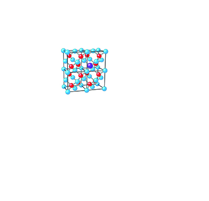
Incorporating bismide (Bi) into gallium arsenide (GaAs) has a dramatic effect on the material band structure (Figure 1).
The dilute bismides research team, led by Dr Robert Richards, is developing the molecular beam epitaxy growth of GaAsBi and related alloys.
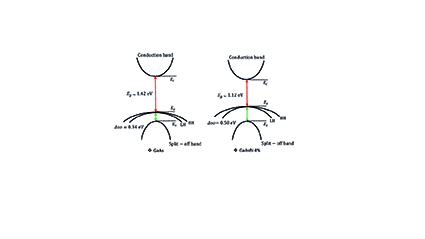
Bi replaces As in the GaAs lattice. The Bi electronic states interact with the valence band edge and cause it to rise rapidly in energy. A few % Bi can cause the valence band edge to rise by hundreds of meV. There are also more sedate changes in the conduction band and split-off band energies. Importantly, this causes a swift increase in the energy difference between the valence and split-off bands; as the spin orbit splits (Δso). Holes must be in the split-off band to acquire enough energy to initiate impact ionisation yet increasing Δso makes it much harder for the holes to reach the split-off band and has the effect of reducing β.
Measuring Bi
According to Dr Richards, the control of Bi on the semiconductor surface is key for the production of GaAsBi devices. “The growth of good quality GaAsBi really comes down to control of the Bi surface layer. As well as providing the Bi, it also acts to smooth the surface and improve the material quality. Too little Bi leaves the surface rough and too much can cause Bi droplets to form. This means carefully selecting the growth temperature and fluxes depending on the Bi content and layer thickness that you want,” he says.
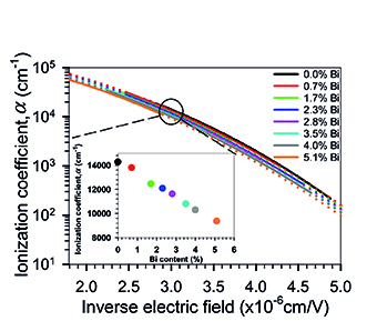
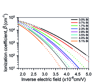 The research team reported the growth and analysis of a series of GaAsBi devices with up to ~5 % Bi, which leads to a significant change of the material’s ionisation properties and extends the material’s absorption cut-off to longer wavelengths than can be achieved by silicon. From detailed opto-electronic characterisation, the α and β coefficients of GaAsBi were calculated at a range of different electric fields and for different Bi contents. As the Bi content is increased, α remains effectively constant, whereas β is reduced by orders of magnitude at low electric fields resulting in a lowering of the excess noise.
Potential uses
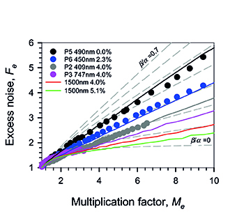
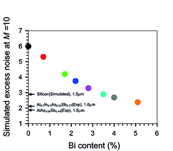 Calculations based on the results suggest that excess noises below those achievable even by silicon are possible with this new material system. Other III-V materials have reached comparably low noise but this performance has never been observed in such a dilute alloy. As the growth of thicker devices containing higher Bi fractions matures, extremely low noise performance throughout the near infrared spectral region should be achievable.
These results promise very low noise APDs, at wavelengths well beyond 1 µm. According to Dr Richards: “Having silicon-like detector properties in a III-V material has been a key goal for a long time. The prospect of this technology providing low noise detectors at wavelengths compatible with telecommunications and lidar is very exciting.”