Electronics Weekly
The technical focus of the collaboration is on advanced packaging and heterogeneous integration of electronic components and systems.
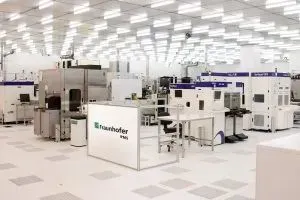
 The Lab-in-Fab model enables efficient development of new processes and technologies in the fields of MEMS, microfluidics, photonics and heterogeneous integration, and their direct transfer into manufacturing.
The innovative technologies’ time span from development to market entry is crucial and an important competitive factor for Europe. This requires new, efficient channels between research institutions and the industry.
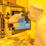
At the heart of the Lab-in-Fab model is a more efficient technology development and its smooth and fast transition to the production environment at X-Fab. This brings research and manufacturing closer together in terms of both content and technology.
When joint customers transition to volume production, missing expertise for scaling new technologies for microelectronics is specifically supplemented or built up. This eliminates the need for additional rounds of development, which significantly reduces the time to market.
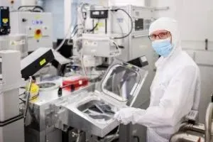
A particular focus of the co-operation is on the joint development of wafer bonding techniques for wafer-level packaging, heterogeneous integration as key technology for future applications in sensing, communication and medical technology, as well as the development of testing and reliability methods.
The co-operation also includes targeted staff exchanges, joint research and funding projects, active participation in technical conferences, and joint market development. This close collaboration not only promotes knowledge transfer but also strengthens the visibility and innovative strength of both partners on the international stage.
The long-standing collaboration between Fraunhofer ENAS and X-Fab reaches a milestone with this model. Customers benefit from an end-to-end service offering: from research and the development of customised technologies to prototyping and volume manufacturing.
”This allows us to develop tailored solutions faster, bring new technologies into production more quickly, while strengthening our customers’ competitiveness,” says X-Fab vice-president Volker Herbig. “Research, development, and mass production are more closely integrated – for the mutual benefit of end customers, Fraunhofer ENAS, and X-Fab.”
A current example of pilot production is the transfer of a complex packaging process for high-precision MEMS sensors in the automotive sector: a screen-printing technology with solder glass pastes developed at Fraunhofer ENAS was successfully integrated into the X-Fab process chain and is now available to customers worldwide as a high-volume foundry service.