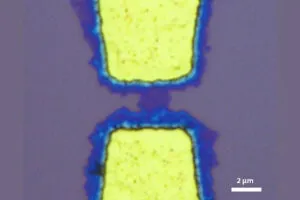
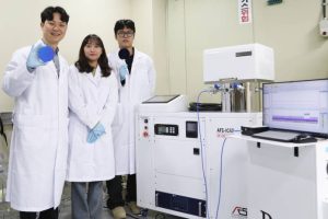
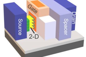
Materials scientists at Rice University have found a way to grow the two-dimensional transition metal dichalcogenide tungsten diselenide directly on patterned gold electrodes and nearby substrate, and demonstrated a transistor. “This is the first demonstration of a transfer-free method to grow 2D devices,” claimed researcher Sathvik Iyengar (pictured). “This is a solid step toward reducing processing temperatures and making a ...
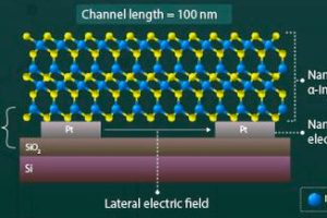
2D material
PECVD makes 2D heterostructures over 100mm wafer
Researchers at the Korea Institute of Machinery and Materials have developed a way to grow 2d transition metal dichalcogenides heterostructures across 100mm wafers using plasma-enhanced chemical vapour deposition (PECVD), claiming this to be a first. “Transition metal dichalcogenides [are] candidates for next-generation semiconductors, with atomic-level 2d structures offering silicon-like performance, low power operation, and fast switching speeds,” according to the ...
2D ferroelectric memory transistor demonstrated
Researchers at Tokyo Tech have made a lateral ferroelectric memory transistor using a 2D material. They picked α-In2Se3, which is “renowned for high carrier mobility, tunable bandgap and strong ferroelectric properties at the atomic level, making it ideal for high-speed memory applications”, according to the university. The bottom-contact transistor has been made by dropping a flake (~29nm thick) of α-In2Se3 ...
Light travels well in few-atom-thick waveguide
The University of Chicago has built optical waveguides only three atoms thick using molybdenum disulphide, and found them to be an efficient way to transfer light over chip-scale distances. “We were surprised by how powerful this super-thin crystal is,” said University of Chicago professor Jiwoong Park, “not only can it hold energy, but deliver it a thousand times further than ...
CEA-Leti and Intel put 2D materials on 300mm wafers for nano-sheet transistors
Intel is to team up with French lab CEA-Leti to put two-dimensional transition-metal dichalcogenides on 300mm wafers. The aim of the multi-year project is to develop a way to transfer layers of 2d material, grown on substrates up to 300mm, to a second substrate for transistor building. Intel will supply manufacturing expertise and CEA-Leti has bonding, layer-transfer and characterisation knowledge. ...
ISSCC 2023: 2D materials instead of silicon in the angstrom era?
At ISSCC 2023 in San Francisco, Belgian research lab Imec presented transistor designs shrunk beyond the capabilities of silicon. It argued that finfet and gate-all-around designs can only go so far with silicon as, to get fast access to the carriers inside a channel, the channels have to be so thin that physics takes its toll. At <3mn, thickness variations ...
Protonic gate spintronics – a tool for low-power ‘electronics’ beyond CMOS?
Electric gate-controlled exchange-bias effect in van der Waals heterostructures has been has observed for the first time, according to RMIT University in Australia, which describes the effect as “a promising platform for future energy-efficient, beyond-CMOS electronics”. “To date, very limited electrically tunable exchange-bias effects have been experimentally demonstrated in some oxide multi-ferroic thin film systems”, according to the university, but ...
Dissimilar 2D materials stack harmoniously to turn photons into electrons
The interfaces in assemblies of 2D materials could produce opto-electronics devices, according to Monash University in Australia, which is designing them using density functional theory (DFT) based band-structure modelling. “2D perovskites show interesting photo-physical properties and better stability compared to typical bulk perovskites,” according to Monash. “However, till now, near-infrared and visible-range optoelectronic device performance metrics of 2D perovskites have ...
p-type 2D transistors mean atomically-thin CMOS is not far away
Van der Waals metal contacts could be the key to CMOS made from thin-film 2D semiconductors, according to the Korea Institute of Science and Technology (KIST), which has made contacts from chlorine-doped tin diselenide. “It was difficult to implement complementary logic circuits with conventional two-dimensional semiconductor devices because they only exhibit the characteristics of either n-type or p-type devices due to ...
That ‘stronger than steel’ polymer
Polymers inside what we call plastics are long thin molecules tangled together – so one-dimensional molecules. Scientists at MIT have managed to make a two-dimensional polymer, which lays down in stuck-together sheets a bit like graphene. The material, dubbed 2DPA-1, has a 2D elastic modulus of ~12.7GPa and a yield strength of ~488MPa, leading MIT to say that these are “between ...
Electronics Weekly