 Electronics Weekly
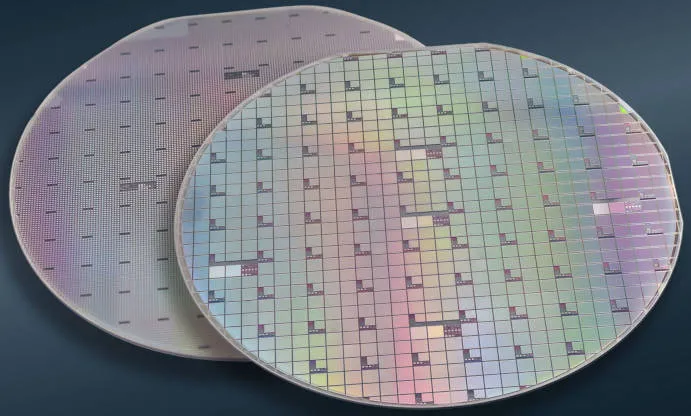
“Developed and manufactured at Onsemi’s fab in Syracuse, New York, Onsemi holds over 130 global patents covering a range of fundamental process, device design, manufacturing and systems innovations for vertical GaN technology,” according to the company. “Compared to commercially available lateral GaN, vertical GaN devices are approximately three times smaller.”
Beyond announcing its existence, the company is revealing little else about this technology, except for claiming: “Vertical GaN leapfrogs both GaN-on-silicon and GaN-on-sapphire devices to deliver higher voltage capability, higher switching frequency, superior reliability and enhanced ruggedness.”
Electronics Weekly requested performance data, and was told that nothing else is being revealed yet.

I couldn’t mention these in a discussion on here a few weeks ago, but there are at least two other companies developing similar products. Not convinced on the frequency claims, but the other claims are very valid and should see GaN displace SiC in a number of applications.
Bulk GaN is not readily available and will be expensive. Thermal conduction is still worse than SiC. Also they’re JFET devices, not MOSFETs so will be more awkward to drive. Niche, if any uptake despite all the marketing muscle behind it.
I would stick to and focus on the long term in-research potential of Ga2O3, Gallium Oxide. Especially since UK groups are focusing on it !!!
Lots of suppliers of bulk GaN wafers. What do you think micro-LEDs are diffused on top of ? Thermal conduction is worse but frequency response and resistivity are better so less losses to create the heat to get rid of. Both are viable solutions for many applications, designers have to choose which is best for their particular implementation.
If you’d read our paper you’d see for long term we’re still backing silicon. And as the longest established semiconductor consultancy in the world our track record is second to none.