Electronics Weekly
And there’s also our roundup of the all latest electronics news from Embedded World 2026 and researchers using high-resolution 3D imaging to detect atomic-scale defects in ICs…
As always, let’s take them in reverse order as according to Google Analytics:
 5. Oracle and OpenAI scrap datacentre project
One of the projects in the $500bn Stargate programne – a datacentre in Abilene, Texas – has been scrapped. The scrapped project was to be an addition to the eight-datacentre Abilene site – two of which have been built with construction proceeding on other datacentres targeted for opening this year. The abandoned project was an extension to the Abilene site being built by Oracle and OpenAI.
4. TSMC to hire 8,000 new people this year
TSMC said at the weekend that it will hire 8,000 more people this year. Engineer recruits with a Masters degree will be paid an average of $70k. The new hires are needed at TSMC’s facilities in Taoyuan, Hsinchu, Miaoli, Taichung, Chiayi, Tainan and Kaohsiung. The disciplines being targeted include electrical engineering, electronics, optoelectronics, physics, materials, and chemical engineering…
 3. Rapidus gets its first customer
Rapidus, Japan’s government-backed leading-edge chip startup, has got its first customer. Canon is going to order 2nm test chips designed by Synopsys to be fabbed at Rapidus’ Chitose site. Last month the company announced that it had raised $1.7bn from 32 private-sector companies (including Canon), with $634m of that coming from the government.
2. Embedded World 2026: Get the full Electronics Weekly Guide
A roundup of the latest electronics news from Embedded World 2026, the major show running from 10-12 March in Nuremberg. The event covers automotive, military, telecoms, industrial and consumer electronics sectors.
 1. Atomic-scale defects discoverable in ICs
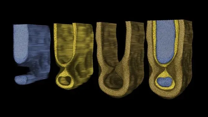
Cornell University researchers have used high-resolution 3D imaging to detect atomic-scale defects in ICs. The imaging method was the result of a collaboration with TSMC and ASM and the research was funded by TSMC. The image below shows the silicon, silicon dioxide and hafnium oxide layers inside a transistor channel. Tiny defects have been a long-standing challenge for the semiconductor industry.