 Electronics Weekly

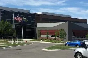
It has increased investment of the facility from $2bn to $7bn across two phases, adding cleanroom space and a a second greenfield packaging and test facility. Amkor Technology said the site will be the first US-based high volume advanced packaging facility and campus, with 750,000 sq ft of cleanroom space.
Arizona’s governor, Katie Hobbs, described the site as an “infrastructure investment” that will create over 3,000 skilled jobs and help build on resilient supply chains and solidify Arizona’s semiconductor leadership”.
The facility will specialise in advanced packaging and test technologies for AI, high-performance computing, mobile applications, communications, and the automotive and industrial sectors.
The company said it evaluated multiple US states and selected Peoria, Arizona “due to its strategic advantages, including proximity to TSMC (the world’s largest silicon foundry). This location enables us to create a robust ecosystem alongside TSMC, Intel, and other industry leaders, leveraging shared educational resources, supplier networks, and technical services”.
At Semicon West, taking place in Phoenix, Arizona this week, David McCann, Amkor’s senior vice president for business units, praised the ‘can do’ attitude and support from the Arizona Commerce Authority, the Greater Phoenix Economic Council and the federal government. The state has attracted semiconductor investment of over $205bn since 2020, including $100bn from TSMC, the largest foreign direct investment.
Advanced packaging market on 9.5% CAGR to reach $79.4bn in 2030


Thanks Caroline. Any more specifics available about what packaging technologies are planned at this site?