Electronics Weekly
The imaging method was the result of a collaboration with TSMC and ASM and the research was funded by TSMC.
Tiny defects have been a long-standing challenge for the semiconductor industry. The game-changer is electron ptychography, a computational imaging method in which an electron microscope pixel array detector (EMPAD) is used to collect detailed scattering patterns of electrons after they pass through the transistors.
By comparing how these patterns change from one scan position to the other, scientists can reconstruct an image with extraordinary clarity. The detector is so precise, it has enabled the highest resolution images in the world.
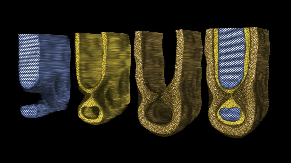
Once the data was collected and reconstructed, and the position of atoms had been tracked, the researchers were able to detect interface roughness in the channels.
The roughness arose from defects that formed during the optimized growth process. Sample structures, grown at nanoelectronics hub Imec, were the ideal way to test the imaging method.
“Fabrication of modern devices takes hundreds, if not thousands, of steps of chemical etching and deposition and heating, and then every single step does something to your structure,” says researcher Shake Karapetyan, “before, you used to look at projective images to try to figure out what was really going on. Now you have a direct probe to actually see after every single step.”