Posted on 26th November 2025 | Modified on 26th November 2025
Manufacturing
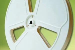
Aiming to reduce environmental load, Osram has teamed up with Zumtobel Group to develop a paper alternative to the plastic reels on which components and LED strips are delivered. “In concrete terms: if Osram were to replace more than half a million plastic reels with paper reels each year, 108 tons of plastic and 436 tons of CO2 emissions could ...
Posted on 19th November 2025 | Modified on 20th November 2025
Business, Finance, Internet of Things, Manufacturing, News, RF & Microwave
Fabless companies are benefitting from CHIPs Act funding, with its impact on the talent pipeline, Jim Guzzo of Impinji told Electronics Weekly. Guzzo, the investment in fabs and the development of fab technology is a driver for investment in STEM, science, technology and manufacturing, he said. The fabless, US company develops its own manufacturing processes. This is partly to protect ...
Posted on 11th November 2025 | Modified on 11th November 2025
Business, Manufacturing
Yangtze Memory Technologies Corp (YMTC) has broken ground on its third NAND fab in Wuhan and plans to run first silicon in 2027, reports the Nikkei. The company is also expanding its second fab and considering entering the DRAM market, say reports. Two years ago YMTC unveiled a 232-layer 3D NAND memory – the X3-9070 – with QLC, ...
Posted on 10th November 2025 | Modified on 10th November 2025
Manufacturing
Stewart Lane is to be president of UK trade body the Manufacturing Technologies Association (MTA). “Stewart brings to the role an exceptional breadth of experience across the technology spectrum,” said MTA CEO James Selka. “Having served on our board since 2016, his understanding of both the technical and strategic dimensions of manufacturing, positions him well to guide the association forward.” ...
Posted on 10th November 2025 | Modified on 11th November 2025
Business, Manufacturing
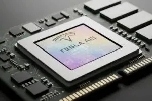
Elon Musk told the Tesla annual shareholders’ meeting last week that he is thinking about making the company vertically integrated by building and operating its own fabs. Showing off his dance moves alongside a dancing Optimus humanoid robot, Musk declared: “I’m super hardcore on chips right now as you may be able to tell. I have chips on the brain. ...
Posted on 29th October 2025 | Modified on 30th October 2025
Manufacturing
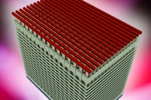
The development of glass-based substrates for electronics in datacentres and high-performance computing is the aim of a consortium gathered by German research institute Fraunhofer IZM (Fraunhofer Institute for reliability and micro-integration). “Due to its material properties, glass offers a promising basis for microelectronics – in particular, its high dimensional stability allows ultra-fine conductor tracks, even below 5μm as structure widths,” ...
Posted on 22nd October 2025 | Modified on 22nd October 2025
Manufacturing, News
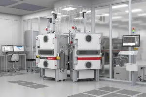
The Opta X300 deposition tool was introduced at Semicon West, marking the Von Ardenne’s entry into the US market. The Opta X300 is purpose-built for high precsion, double-side deposition to support “the most demanding multilayer applications,” said Guideo Ueberreiter, vice president of semiconductor strategy at Von Ardenne. The rotary disk coating system is designed for sub-nm precision deposition on and ...
Posted on 21st October 2025 | Modified on 21st October 2025
Manufacturing
Segger has announced an industrial-grade 13 port USB-C hub. Called USB Hub-13, it is an extension of the company’s earlier USB Hub-7. “USB Hub-13 is an ideal partner for gang-programming setups,” claimed the company marketing head Dirk Akemann. “Like its predecessor, it was designed from the ground up to pair well with other products in our programming ecosystem.” To protect ...
Posted on 20th October 2025 | Modified on 20th October 2025
AI, Automotive Electronics, Manufacturing, News
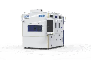
The Ultra ECDP (electrochemical deplating) tool is designed specifically for wide bandgap compound semiconductor manufacturing, said ACM Research. It delivers uniform processing outside of the wafer pattern area with minimal undercut for high-precision wafer level gold (Au) bump, thin film and deep hole deplating. Gold exhibits high conductivity, corrosion resistance and malleability and is emerging as an advantageous material for ...
Posted on 17th October 2025 | Modified on 22nd October 2025
Business, Manufacturing
Samsung is reported to be paying $773m for two high-NA EUV machines – the Twinscan EXE:5200B – with one for delivery this year and one for delivery in H1 2026. Samsung already has a high-NA EUV tool for R&D use at its Hwaseong facility, which is where the two new high-NA machines will also be installed. The two machines will ...
 Electronics Weekly