Posted on 5th February 2026 | Modified on 5th February 2026
AI, Analogue / Linear / Mixed Signal ICs, Business, Communications, Digital Integrated Circuits, Microprocessors, News, Process R&D, Products, Sensors
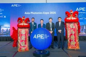
The importance of Singapore as a technology hub was reinforced today at the opening of the Asia Photonics Expo (APE) 2026. This year’s APE (4-6 February) is at Sands Expo and Convention Centre, Singapore. The three-day conference and exhibition will host more than 350 exhibitors, from 17 countries and regions and expects to welcome 6,000 guests from 50 countries. “The ...
Posted on 23rd December 2025 | Modified on 23rd December 2025
Business, Device R&D, Materials R&D, News, Process R&D, Research, University Electronics
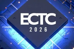
A competition launched by the IEEE offers six student teams the chance to attend next year’s Electronic Components and Technology Conference in Orlando, Florida. There are three challenges, each dealing with a critical aspect of simulation and reliability in electronic packaging. The first is for BSc and MSc students: to define a low-cost robust thermal solution for a high power ...
Posted on 10th October 2025 | Modified on 13th October 2025
AI, Manufacturing, Military/Aerospace Electronics, News, Process R&D
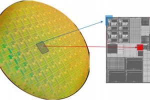
A hyper-beam array lithography system has been introduced to the US, based on architecture pioneered in Europe. The lithography tool operates with 65,000 independently controlled parallel beams which delivers capabilities at a scale no electron beam technology can match, said the company. Installed at Northrup Grumann, it addresses the holy grail of chip design, said founder and CEO, Lex Keen. ...
Posted on 18th November 2020 | Modified on 18th November 2020
Automotive Electronics, Business, Design, Device R&D, Embedded Systems, Industrial Electronics, Internet of Things, Markets, Military/Aerospace Electronics, News, Process R&D, Research
EDA company, Mentor, has joined Nano 2022, the latest project to promote the French electronics manufacturing industry. It covers components, connectors and PCBs, to design and assembly, distribution, embedded software and software tools. The project is part of the European Commission’s Important Project of Common European Interest (IPCEI) to promote research and innovation in power ICs, sensors, optical equipment and ...
Posted on 13th April 2018 | Modified on 13th April 2018
News, Process R&D
New inks for inkjet printers make it possible to print organic displays or solar cells on film and glass for the use in architecture, the textile industry and many other industries, according to the Fraunhofer Institute for Applied Polymer Research IAP. At Printed Electronics Europe in Berlin this week, Fraunhofer IAP demonstrated how inks can be printed on solid substrates ...
Posted on 8th March 2018 | Modified on 8th March 2018
News, Process R&D
Leti, the French microelectronics research centre, says it has developed a way to encrypt individual chips with a security code. Working with lithography equipment supplier Mapper Lithography, Leti says it has perfected a way to generate a non-falsifiable code using a new chip design that leverages direct multi-beam writing in a process that fits in a conventional CMOS flow with ...
Posted on 25th January 2018 | Modified on 23rd June 2025
News, Power Supplies, Process, Process R&D
Continuing the industry’s love affair with lithium for batteries, researchers have found a way to avoid dendrites which grow on as the battery charges and discharges and which can degrade performance. Building on work began by Jiaxing Huang, professor of materials science and engineering at Northwestern University’s McCormick School of Engineering, Jiayan Luo, professor of chemical engineering at Tianjin University ...
Posted on 7th December 2017 | Modified on 8th December 2017
News, Process R&D
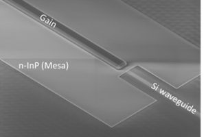
French research group Leti has demonstrated a III-V semiconductor fabrication technique which it says will simplify the production of lasers. Leti says it has integrated hybrid III-V silicon lasers on 200mm wafers using standard CMOS process flow. “This shows the way to transitioning away from 100mm wafers and a process based on bulk III-V technology that requires contacts with noble ...
Posted on 22nd November 2017 | Modified on 23rd November 2017
News, Process R&D, University Electronics
CST Global, the Glasgow-based III-V opto-electronic, semiconductor foundry, is collaborating with the University of Glasgow and Gas Sensing Solutions on a project to fabricate active matrix, single-photon GaAs devices. The project will develop light-weight, monolithic, mid-wave infrared (MWIR) imagers, capable of detecting a single photon of IR light. These are primarily used to image gasses and diagnose their composition. Dr ...
Posted on 14th November 2017 | Modified on 14th November 2017
News, Process R&D
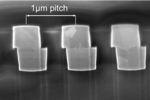
Leti, an institute of CEA Tech, has announced the world’s first successful 300mm wafer-to-wafer direct hybrid bonding with pitch dimension connections as small as 1µm and copper pads as small as 500nm. This was achieved in partnership with EV Group, a supplier of wafer bonding and lithography equipment. “To our knowledge, this is the first reported demonstration of sub-1.5µm pitch ...
 Electronics Weekly